Quantcast
Channel: EFY Bureau – Electronics For You
Viewing all 5950 articles
Browse latest View live

Vodafone India to Launch VoLTE In January 2018

$
0
0
  • Vodafone VoLTE will be available across India, starting with Karnataka, Mumbai, Gujarat, Delhi, and Kolkata
  • HD quality voice calls along with faster call set up time
  • Vodafone SuperNet 4G customers will experience VoLTE (Voice over LTE) services for free

Vodafone, one of India’s largest telecommunication services provider, confirmed the roll-out of its VoLTE services beginning January 2018. In the first phase, Vodafone VoLTE service will be available in Karnataka, Mumbai, Gujarat, Delhi, and Kolkata and will be extended across the country in a short time.

Vodafone’s VoLTE services will allow Vodafone SuperNet 4G customers to experience HD quality crystal clear voice with super call connect time. Vodafone 4G customers will experience VoLTE at no additional charges. All they need is a handset supporting Vodafone VoLTE and a 4G SIM.

Announcing Vodafone VoLTE service, Sunil Sood, Managing Director and Chief Executive Officer, Vodafone India, said, “Vodafone is getting Future Ready with the advent of newer technologies and digital services. The introduction of Voice over LTE (VoLTE) will enhance customer experience with HD quality calling and offer our customers newer possibilities. Vodafone VoLTE is an important step towards introducing futuristic technology enhancing our Data Strong Network.”

Using the latest technological developments Vodafone has built a robust and resilient Data Strong Network of ~140,000 sites that enable better call quality and mobile internet experience to its customers. This will be a key differentiator for Vodafone in providing seamless connectivity and experience to its customers.


The post Vodafone India to Launch VoLTE In January 2018 appeared first on Electronics For You.


New AP7381 Voltage Regulator With Ultra-Low Quiescent Current and High Accuracy

$
0
0

Diodes Incorporated, a leading global manufacturer and supplier of high-quality application specific standard products within the broad discrete, logic, analog and mixed-signal semiconductor markets, today introduced the AP7381. Operating from a wide input voltage spanning 3.3V to 40V, this positive voltage regulator offers ultra-low quiescent current and high accuracy, making it well-suited for use in a variety of applications ranging from USB and portable devices to energy meters and home automation.

The AP7381 is offered with fixed output voltages of 3.3V or 5V to power standard logic device supplies and I/O levels and can operate from an input voltage between 3.3V and 40V, which covers most common system power rails. The device provides excellent line and load regulation and features a low dropout voltage of typically 1000mV for a 3.3V output device operating at an output current of 100mA. An internal voltage reference ensures output accuracy at room temperature is maintained within ±2%.

A low quiescent current of just 2.5µA minimizes standby power in low-power systems and extends the life of battery-operated products. The AP7381 has a built-in current limit and an over-temperature protection (OTP) function and also features over-current protection, provided by an internal current limit circuit.


The post New AP7381 Voltage Regulator With Ultra-Low Quiescent Current and High Accuracy appeared first on Electronics For You.

The Best Wi-Fi Router For Your Office

$
0
0

If you run a small business, it is advisable to hand-pick your own Wi-Fi router. While the router provided by your Internet service provider may be authentic, it might not be the right fit for your business. Routers across the globe have come a long way with significant improvements in speed capabilities, security and signal strength consistency. Router speed, signal strength and bandwidth are the key priorities for home offices. However, small businesses require a few more features as an integral part of the setup. You need to find the best wi-fi router for your needs.

WPA2 AES security

Not familiar with the jargons WPA or AES? Let us explain. Wi-Fi Protected Access (WPA) is a wireless network security protocol. For small offices or home office setups, WPA2 utilising 128-bit Advanced Encryption Standard (AES) with pre-shared key (PSK) encryption compatibility is the most popular as well as preferable algorithm with disabled Wi-Fi Protected Setup (WPS). Bigger businesses go for WPA2-Enterprise, also known as RADIUS security protocol, which provides the best level of security. But the associated cost, infrastructure and maintenance requirements might not make it feasible for a small business arrangement. Other than this, good practices and security measures like active internal firewall and updated firmware can enhance the network safeguard.

Extra ports

Home routers usually come with four 10x100Mbps LAN ports and one WAN port. Small businesses should look for routers with extra ports. Else, they can pick a switch to expand their networks. To expand bandwidth or ensure a working port as a backup for connectivity if the main WAN malfunctions, look for extra WAN ports to connect additional service from your ISP. That way, you can balance the load on the network when your business supports a bigger employee base.

multiple antenna on router

Dual band to avoid network jamming

Networks get painfully slow when buffering a video or opening a heavy website. That happens due to cluttering of network channels. Single-band Wi-Fi routers function at a bandwidth frequency of 2.4GHz, which provides a good coverage range; the higher the frequency value, the lower the range. But this specific bandwidth is also tapped in by other gadgets like phones and tablets. Lower channel width is jammed by multiple devices, which causes the 2.4GHz bandwidth to clutter faster. Therefore high-volume data streaming becomes slow for single-band routers.

Dual-band routers can tap into two frequency bandwidths: 2.4GHz and 5GHz. While 5GHz bandwidth provides much smaller coverage area, the wider data channel allows it to transmit much larger volumes of data. Latest dual-band routers divide their data flow—maintaining the lower-volume data through the 2.4GHz frequency, while routing the higher data volume, for example in video stream or gaming, through the 5GHz frequency.

what you need

Latest 802.11 standard for best wi-fi router

The IEEE Standards Association has introduced Wi-Fi standards for high network throughput. The most efficient standard at the moment is 802.11ac, which supports data throughput (data transmission rate) up to 2Gbps (depending on the number of spatial streams, each of which carries around 433Mbps of data), wireless range up to 61 metres (200 feet), and four wireless channels of 20MHz, 40MHz, 80MHz and 160MHz widths. Additionally, the 802.11ac (also known as 11ac) standard taps into the 5GHz bandwidth, avoiding clustered or jammed network. The cost, however, is also more.

The most popular category till now, keeping in mind the cost, is the 802.11n standard (also denoted as 11n), which can offer data throughput of up to 600Mbps (considering four spatial streams, each supporting 150Mbps). It supports wireless range of up to 122 metres (400 feet) and two channel widths of 20MHz and 40MHz, and functions in the 2.4GHz bandwidth. While 11ac is the recommended Wi-Fi standard, the choice largely depends on your budget.

LAN and WAN ports of a router (Image courtesy: wikimedia commons)

LAN and WAN ports of a router (Image courtesy: wikimedia commons)

More antennae and MU-MIMO for stronger network

The number of antennae on a router indicates the spatial streams (or channels) of data transmission. Each antenna in a router comprises a single transmitter and a single receiver end, and has a notation of its own: 1×1 implies a single antenna with one transmitter and one receiver, and is called a single-input single-output (SISO) system; 2×2 implies two antennae, each with one transmitter and one receiver, and is called a multiple-input multiple-output (MIMO) system.

Routers with a single antenna can transmit data through a single spatial stream—correlating to the 2.4GHz bandwidth. As discussed earlier, in that case, most electronic devices have a chance of interference, causing the network to slow down. 2×2 routers can tap into two spatial streams. In 11n standard routers, both antennae support 2.4GHz bandwidth, attaining a throughput of up to 300Mbps (considering each stream supports 150Mbps data at 2.4GHz). In comparison, in 11ac standard 2×2 routers, one stream taps into the 5GHz bandwidth, while the other works at 2.4GHz, greatly reducing the cluttering and increasing the data transmission rate from 600Mbps up to 1Gbps.

The post The Best Wi-Fi Router For Your Office appeared first on Electronics For You.

IIoT to PCB layout: Open Source has More than What You Need!

$
0
0

The following software, besides other, can be found in the DVD accompanying EFY Plus edition of this magazine

TinyCAD 2.8

TinyCAD is a handy PCB layout and circuit schematic tool with a vast library of components. It lets you create your own customised symbols too. TinyCAD is similar to all the other PCB software that are not open source. It provides you facilities ranging from building symbols to adding texts and annotations, buses and power signals, and symbol attributes to editing of drawings. Its newer version, 2.8, is even better with all new upgrades.

AdvancedHMI

This easy-to-use software lets you create human-machine interfaces (HMIs) that are not possible with other off-the-shelf packages. It requires popular Visual Studio and is based on .NET framework. The best part of this freeware is that the user need not know the complicated coding for its execution as it has a drag-and-drop option. It is SCADA capable, and supports Omron and Allen Bradley DF1 RS232 drivers. It is tested on Mono on Linux, and even works on Raspberry Pi.

Shotcut

Shotcut video editing software supports various kinds of video and audio formats. It supports native editing (no import required), multi-format timelines, resolutions and frame-rates in the same project. It is used for screen, webcam and audio capture too. It supports resolutions up to 4k and capture from X11 screen and Windows DirectShow devices. It also supports drag-n-drop of assets from file manager.

Thunderbird

There are several e-mail applications available online, but Mozilla Thunderbird is one of its kind and user-friendly software used since long. It combines the benefits of security, speed and latest technology together in one frame. Mozilla Thunderbird is easy as it can be accessed after the mail wizard setup is installed. It is loaded with features like one-click access book, a reminder attachment, multiple-channel chat and personalised e-mail address.

iDempiere

It is an open source ERP software for enterprises. Thus, customer relationship management and supply chain management are its key elements. With enhanced features, iDempiere supports multiple tenants, multiple organisations, multiple language support, multiple currencies and multiple account schemas. It consists of a Java-based server that allows management of entities, validation rules, windows, formats and other customised applications without a new Java code.

LibrePlan 1.4

This free collaborative tool for project management is designed to meet the needs of organisational complexities and production processes. It lets users plan, monitor, control and organise tasks and projects. Its rich web interface provides a desktop-like user experience.


The post IIoT to PCB layout: Open Source has More than What You Need! appeared first on Electronics For You.

Which Microscope to use for SMD Soldering?

Industry’s First FPGA Integrated with High Bandwidth Memory Built for Acceleration

$
0
0

December 18, 2017 – Intel today announced the availability of the Intel Stratix 10 MX FPGA, the industry’s first field programmable gate array (FPGA) with integrated High Bandwidth Memory DRAM (HBM2). By integrating the FPGA and the HBM2, Intel Stratix 10 MX FPGAs offer up to 10 times the memory bandwidth when compared with standalone DDR memory solutions. These bandwidth capabilities make Intel Stratix 10 MX FPGAs the essential multi-function accelerators for high-performance computing (HPC), data centers, network functions virtualization (NFV), and broadcast applications that require hardware accelerators to speed-up mass data movements and stream data pipeline frameworks.

In HPC environments, the ability to compress and decompress data before or after mass data movements is paramount. HBM2-based FPGAs can compress and accelerate larger data movements compared with stand-alone FPGAs. With High Performance Data Analytics (HPDA) environments, streaming data pipeline frameworks like Apache* Kafka and Apache* Spark Streaming require real-time hardware acceleration. Intel Stratix 10 MX FPGAs can simultaneously read/write data and encrypt/decrypt data in real-time without burdening the host CPU resources.

“To efficiently accelerate these workloads, memory bandwidth needs to keep pace with the explosion in data” said Reynette Au, vice president of marketing, Intel Programmable Solutions Group. “We designed the Intel Stratix 10 MX family to provide a new class of FPGA-based multi-function data accelerators for HPC and HPDA markets.”

The Intel Stratix 10 MX FPGA family provides a maximum memory bandwidth of 512 gigabytes per second with the integrated HBM2. HBM2 vertically stacks DRAM layers using silicon via (TSV) technology. These DRAM layers sit on a base layer that connects to the FPGA using high density micro bumps. The Intel Stratix 10 MX FPGA family utilizes Intel’s Embedded Multi-Die Interconnect Bridge (EMIB) that speeds communication between FPGA fabric and the DRAM. EMIB works to efficiently integrate HBM2 with a high-performance monolithic FPGA fabric, solving the memory bandwidth bottleneck in a power-efficient manner.

Intel is shipping several Intel Stratix 10 FPGA family variants, including the Intel Stratix 10 GX FPGAs (with 28G transceivers) and the Intel Stratix 10 SX FPGAs (with embedded quad-core ARM processor). The Intel Stratix 10 FPGA family utilizes Intel’s 14 nm FinFET manufacturing process and incorporates state-of-the-art packaging technology, including EMIB.


The post Industry’s First FPGA Integrated with High Bandwidth Memory Built for Acceleration appeared first on Electronics For You.

New All-in-one Software Tool Makes STM32 Microcontroller Programming More User-Friendly

$
0
0

Geneva / 21 Dec 2017: STMicroelectronics’ STM32CubeProgrammer (STM32CUBEPROG) software tool delivers device-programming and firmware upgrade for STM32 microcontrollers in a unified, multi-platform, and user-configurable environment.

Ready to run on Windows, Linux, or MacOS operating systems, the STM32CubeProgrammer can program the STM32 microcontroller’s on-chip Flash/RAM or external memories using various file formats. Further capabilities include whole-memory or sector erase and programming microcontroller option bytes. Users can also generate encrypted files for secure programming (Secure Firmware Install/Update) to authenticate production and protect intellectual property.

With this universal tool, users can program STM32 microcontrollers through the device’s SWD (Single-Wire Debug) or JTAG debugging ports, or the bootloader ports (such as UART and USB). Hence the STM32CubeProgrammer brings the individual capabilities of the ST Visual Programmer, DFUse Device Firmware Update tool, Flash Loader, and ST-Link utility together within the STM32Cube ecosystem. ST will extend the STM32CubeProgrammer’s capabilities by adding programming access via microcontroller I2C and CAN ports.

Furthermore, the STM32CubeProgrammer provides many opportunities to customize and configure features, using either the Graphical User Interface (GUI) or the Command-Line Interface (CLI). Also, this all-in-one tool can be used in standalone mode or integrated and controlled from a custom application. Programming can be done manually or automated using scripts.


The post New All-in-one Software Tool Makes STM32 Microcontroller Programming More User-Friendly appeared first on Electronics For You.

Password-Protected Bluetooth Remote Control

$
0
0

This password protected bluetooth based remote control operating at 2.4GHz frequency can be used to control robots, home appliances, machines, etc. Here we have used the secure remote to control a war robot that has three motors, one of which is used to lift objects or weapons such as a cutter (or sword). The article describes configuration of the remote control system and doesn’t cover construction and working of the robot in detail due to paucity of space.

Circuit and working

The project consists of two pairs of Arduino and Bluetooth HC-05 modules, one of which is used in the transmitter unit and the other in the receiver unit. The Bluetooth module on the transmitter side is configured as master, while the module on the receiver side is configured as slave. The author’s prototypes for the transmitter unit and the receiver unit are shown in Figs 1 and 2, respectively.

author's prototype of the transmitter unit

Fig. 1: Author’s prototype of transmitter unit

author's prototype of the receiver unit

Fig. 2: Author’s prototype of receiver unit

Transmitter unit

Circuit diagram of the transmitter unit is shown in Fig. 3. The prototype uses six pushbuttons/switches (S1 through S6), which are connected to the Arduino board (Board1) using jumper wires. All these switches are used to control the motors for different movements of the robot. The HC-05 Bluetooth module (BT1) is also connected to Board1 as shown in Fig. 3.

Bluetooth based remote control: transmitter unit circuit

Fig. 3: Circuit diagram of transmitter unit

Receiver unit

Circuit diagram of the receiver unit is shown in Fig. 4. It consists of Arduino board (Board2), HC-05 Bluetooth module (BT2), six 12V, 1CO relays (RL1 through RL6), three DC motors (M1, M2 and M3), six relay driver transistors 2N2222 (T1 through T6) and a few other components. The author’s prototype uses a 4-channel relay card for the robot’s right and left wheels and a 2-channel relay card to drive the motor for lifting the object. BT2 is connected to Board2 using jumper wires. All the relay cards are connected to Board2.

Bluetooth based remote control: receiver unit circuit

Fig. 4: Circuit diagram of receiver unit

The relay card should be made as per your requirement. In this tutorial, circuit is used to drive a robot using DC motors. So two relays are used to run a motor in both directions.

Switches S1 through S6 in the transmitter unit work as the remote control buttons, which send digital signals to the receiver unit through Board1 and BT1.

The signals from the transmitter unit are received by BT2 in the receiver unit and forwarded to Board2 for processing. Since relay boards are connected to digital output pins of Board2, the relay energises or de-energises as per the status of signals available on digital output pins.

Relays

Relays at the receiver side are used to drive the motors in the desired directions through Arduino Board2. Relay drivers include the combination of a transistor and a diode as shown in Fig. 4. You can use higher-power-rating relays for driving heavy DC motors. In the prototype, the author has used 12V DC, 8-pin JQX-30F power relays by removing sugar-cube PCB relays from the relay cards. Proper combination of relays and contacts makes the motors run in the desired directions.

Pairing of Bluetooth modules

HC-05 modules of the transmitter and the receiver are to be paired first before using them in the project. The process to configure the HC-05 modules is explained below.

To pair two HC-05 modules, you need an Arduino board and a USB-to-UART adaptor like CP2102 converter. An HC-05 module can be configured to work either in slave or master mode.

Configuring slave module. Connections between HC-05 and Arduino are shown below:

HC-05 (BT2) Arduino (Board 2)
Rx Rx
Tx Tx
GND GND
Vcc Vcc
Key 3.3V


In order to enter ‘attention’ (AT) command mode of HC-05, a null program is required in the Arduino board. (AT commands are Hayes command set commonly used in modem and serial communications.) The key pin of HC-05 must be connected to 3.3V in order to enter AT command mode.

After proper connections, check the baud rate of your HC-05 module. Configure the baud rate to 38400. Upload the following null program to Arduino board:

void setup()
{

}

void loop()
{
}

After uploading the program, start ‘Serial Monitor’ in Arduino IDE. Select ‘Both NL & CR’ and ‘Baud rate as 38400’ in ‘Serial Monitor’ window.

To know details of the current HC-05 device, just type AT+NAME in the edit box in ‘Serial Monitor.’ To change the device to the desired name, say, Tej Patel, type AT+NAME= Tej Patel

To change password of the module, enter the following command:

At+PSWD=*****

where ***** can be any character string, say, efy12

To configure the module in slave mode, type AT+ROLE=0

Every Bluetooth module has its own address. To know the current device address, type AT+ADDR

Here, the address is 98d3:31:305f7b

Replace colons with commas as given below:
AT+LINK=98d3,31,305f7b

And note down this address because you will need this later on while configuring the master module (BT1). Now, you may disconnect the power and remove the key pin from the module.

The post Password-Protected Bluetooth Remote Control appeared first on Electronics For You.


Three Phase Appliance Protector

$
0
0

Many of our costly appliances require three-phase AC supply for operation. Failure of any of the phases makes the appliance prone to erratic functioning and may even lead to failure. Hence it is of paramount importance to monitor the availability of the three-phase supply and switch off the appliance in the event of failure of one or two phases. The power to the appliance should resume with the availability of all phases of the supply with certain time delay in order to avoid surges and momentary fluctuations.

Three phase appliance protector

The complete circuit of a three phase appliance protector is described here. It requires three-phase supply, three 12V relays and a timer IC NE555 along with 230V coil contactor having four poles.

Three Phase Appliance Protector Circuit

Relays RL1 and RL2 act as a sensing devices for phases Y and B, respectively. These relays are connected such that each acts as an enabling device for the subsequent relay. Therefore the combination of the relays forms a logical AND gate connected serially.

Circuit operation

The availability of phase R energises relay RL1 and its normally-opened (N/O) contacts close to connect phase Y to the input of transformer X2. The availability of phase Y energises relay RL2 and its N/O contacts close to connect phase B to the input of transformer X3, thus applying a triggering input to timer IC NE555 (IC1).

Therefore the delay timer built around NE555 triggers only when all the phases (R, Y and B) are available. It provides a delay of approximately four seconds, which energises relay RL3 and its N/O contact closes to connect the line to the energising coil of four-pole contactor relay RL4. Contactor RL4 closes to ensure the availability of the three-phase supply to the appliance.

The rating of contactor RL4 can be selected according to the full-load current rating of the appliances. Here the contact current rating of the four-pole contactor is up to 32A. The availability of phases R, Y and B is monitored by appropriate LEDs connected across the secondary windings of transformers X1, X2 and X3, respectively. Hence this circuit does not require a separate indicator lamp for monitoring the availability of the three phases. When phase R is available, LED1 glows. When phase Y is available, LED2 glows. When phase B is available, LED3 glows.

The main advantage of this protector circuit is that it protects three-phase appliances from failure of any of the phases by disconnecting the power supply through the contactor and automatically restores the three-phase supply to the appliance (with reasonable time delay) when all the phases are available.

Construction & testing

Assemble the circuit on a general purpose PCB and enclose in a cabinet with the relays and contactor mounted on the backside of cabinet. Connect the appliance through external wires.

Caution

To avoid the risk of electric shock, ensure that AC mains is disconnected during assembly of the circuit and double check everything before connecting your circuit to the mains.


The article was first published in August 2008 and has recently been updated.

The post Three Phase Appliance Protector appeared first on Electronics For You.

Electronic Combination Lock

$
0
0

This 7-digit electronic combination lock can be easily hard-wired for any combination that you choose. The circuit uses a 4-bit, divide-by-8 Johnson counter (IC1), ten push button switches and NPN transistor T1.

Electronic combination lock circuit

At power ‘on,’ capacitor C2 connected to pin 15 of IC1 charges to high level through 820-kilo-ohm resistor, holding the counter in the reset state. In this condition, output O0 (pin 2) of counter IC1 is high, while all other outputs are low.

Electronic combination lock circuit
Fig. 1: Electronic combination lock circuit

Circuit operation

When switch S2 is pressed, transistor T1 conducts and capacitor C2 discharges via diode D1 and resistor R2, releasing the counter’s reset input. When S2 is released, T1 cuts off and its collector is pulled high, generating a rising edge on the counter’s input clock pin 14. Capacitor C1 and resistor R3 in the base circuit of transistor T1 form a simple filter to prevent switch contact bounce from generating multiple clock pulses on pin 14 of IC1.

The clock pulse advances IC1’s count by one, so O0 goes low and O1 goes high. Therefore press switch S7 next, as it’s wired to output O1. The time required for capacitor C1 to charge to logic high level is the maximum time that can lapse between switches pressed. Otherwise, the counter will reset. When all switches have been pressed in the correct sequence (S2-S7-S3-S4-S5-S2-S2 as shown), output O7 (pin 10) of the counter goes high for about ten seconds. This output is fed to driver transistor T2 to drive the solenoid valve and open the lock.

Pin configurations of BC548 and BD139

Construction & testing

Assemble the circuit on a common PCB and enclose in a plastic cabinet. Connect the solenoid valve to the circuit using a flexible wire. While soldering, take care to avoid shorting. Use IC base for ease of troubleshooting. Connect the switches for opening the lock at the top of the plastic case.


The article was first published in November 2008 and has recently been updated.

The post Electronic Combination Lock appeared first on Electronics For You.

Program Arduino With Your Android Device

$
0
0

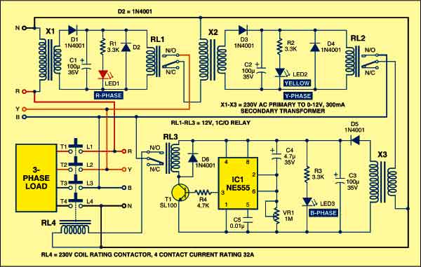
As you may already know, using a USB OTG (on-the-go) adaptor, you can connect pen drives, game controllers, etc to your Android device. This adaptor can also be used to power small devices like Arduino boards from Android devices.

However, given the processing power of today’s Android mobile devices, these could be used to do much more than just powering up Arduino prototypes. Realising this, Anton Smirnov created a full-fledged Arduino IDE for Android. Called ArduinoDroid, it has features almost identical to those of IDEs available for PC, and even better in some cases. This article explains how you can program an Arduino board using ArduinoDroid app on your Android device like a smartphone or tablet.

Requirements

To get started, you need an Arduino board, an Android phone that supports USB OTG and has ArduinoDroid app installed on it, and OTG cable. Most of the necessary features like open/edit Arduino sketches, libraries and example sketches, code syntax highlighting, compile sketches and upload sketches are available in the free version of ArduinoDroid app. But if you don’t want advertisement banners, colour themes and non-essential features like dropbox support, smart engine and smart keyboard, the paid version is the way to go.

Interface

Interface is pretty clean, not cluttered with tabs and buttons. Top row consists of icons of essential features like save, compile, download and console (serial monitor) as shown in Fig. 1. Then around 50 per cent of the screen area is allocated to Editor and Navigator on the upper side and Diagnostics and Output windows on the bottom side.

Essential icons of ArduinoDroid app

Fig. 1: Essential icons of ArduinoDroid app

How it works

Write/modify your desired sketch in Editor section as shown in Fig. 2.

Arduino Editor

Fig. 2: Editor

Compile it by pressing the icon next to save icon. Wait for a while, it might take some time, depending on your sketch and the mobile device. Then check the output section at the bottom for any error/warning as shown in Fig. 3.

Fig. 3: Output section

If there is no error, you can upload your sketch on the Arduino board.

Connect Arduino to your mobile device using USB OTG. Select the desired board from the options under SettingsBoard type (as shown in Fig. 4, where Arduino Duemilanove with ATmega328 option is selected).

Fig. 4: Selecting the Arduino board

Now click ‘Upload’ to upload the sketch into Arduino.


The post Program Arduino With Your Android Device appeared first on Electronics For You.

“There is an Ongoing Requirement for Higher-Performance Power Systems”

$
0
0

All electronic products have power management systems, designing which is a common challenge faced by designers. Recently, Vicor initiated a global survey to understand various aspects of power system design. To understand the survey findings, Rahul Chopra and Sneha Ambastha from EFY spoke to Andy Gales, vice president, Vicor.


 Andy Gales, vice president, Vicor
Andy Gales, vice president, Vicor


Q. Do you see Indian companies taking leadership role in power supply design?

A. I think it’s already happening and ‘Make in India’ is the primary example. You have a wide range of engineers in India. Previously, countries like India used to procure power supplies from the US and Europe. However, now they have started designing solutions here themselves.

Q. How important is power supply design in the overall product design cycle?

A. Power supply design is one of the goals but there are other associated tasks too. We found that engineers are commonly multitasking, so often they have more than one power project on the go at a time. Thus, they are not just designing one solution but may be several, for multiple customers. We also found that design engineers are commonly required to develop other parts of the product, sometimes even the software for a new user interface. As a result, very often in these companies, the team building power supplies may not be expert.

In such cases, modular solutions can help them deliver better performance. They don’t need to understand details like switching topologies used inside the black box. They can trust the datasheets and rely on the power components to get the performance they require.

Q. How can design engineers achieve higher-performance solutions?

A. There is an ongoing requirement for higher-performance power systems. Achieving high performance from a few resistors, capacitors and FETS can be a struggle without the right expertise. However, if you base the design on power components, which are already optimised for size or efficiency, you can plug these into a circuit board and quickly provide a solution that is close enough to meet the desired product specifications.

Q. What are the common challenges in design engineering?

A. Education. We need to educate engineers to understand the issues faced in using these components, whether it’s meeting EMI/transient input specifications or managing heat. Having the right knowledge is critical for success.

At Vicor, we offer a design review for the common problems that we have seen in the past for power applications. So from the design point of view, we make sure that the customer ends up with a solution that stands the test of time.

Q. What resources are available to help design engineers?

A. Making engineers aware of the best practices and the tools available will help them to get their solution right first time. At Vicor, we have a number of design resources on our website, including our power system designer that helps optimise solutions for size, efficiency or cost. The website also has simulators and whiteboards for estimating the final system performance before you prototype, as well as application notes that cover common issues. We also host seminars and webinars to help engineers understand our technology better.


The post “There is an Ongoing Requirement for Higher-Performance Power Systems” appeared first on Electronics For You.

New Three-phase MOSFET Driver IC with On-board Regulator

$
0
0

Used to Supply both Sensors and Microprocessor Power

Worcester, MA – January 2, 2018– Allegro MicroSystems, LLC announces a new three-phase MOSFET driver IC with an integrated low dropout regulator supplying 5 V or 3.3 V. Allegro’s A4919 is designed for a wide range of industrial applications. It can be controlled with block (trapezoidal), sinusoidal, or vector commutation when interfaced with a microprocessor. The A4919 is designed to be a simple direct control gate driver for both the commercial and industrial markets providing LDO for peripherals or a microprocessor and provide complete flexibility over commutation.

A unique charge pump regulator provides full (>10 V) gate drive at power supply voltages down to 7 V and allows the A4919 to operate with reduced gate drive at power supply voltages down to 5.5 V. A bootstrap capacitor is used to provide the above power supply voltage required for the high side N-channel MOSFETs. One logic-level input is provided for each of the six power MOSFETs in the three-phase bridge, allowing motors to be driven with any commutation scheme defined by an external controller. The power MOSFETs are protected from cross-conduction by integrated crossover control.

Motor phase short-to-supply and short-to-ground detection is provided by independent drain-source voltage monitors on each MOSFET. Short faults, supply undervoltage, and chip overtemperature conditions are indicated by a single open-drain fault output. Product variants include either 5.0 V or 3.3 V LDO or an option without LDO and instead provides a voltage input which can be used to monitor an external voltage source.

The A4919 is supplied in a 28-pin TSSOP power package (package type LP) and a 28-terminal 5 mm × 5 mm × 0.90 mm (QFN package) both with an exposed pad for enhanced thermal performance. Both packages are lead (Pb) free, with 100% matte-tin leadframe plating (suffix T).

Pricing in quantities of 1,000 are as follows:

  • A4919GLPTR – $2.60
  • A4919GLPTR-5-T – $2.85
  • A4919GLPTR-3-T – $2.85
  • A4919GETTR-T – $2.30
  • A4919GETTR-5-T – $2.39
  • A4919GETTR-3-T – $2.39

The post New Three-phase MOSFET Driver IC with On-board Regulator appeared first on Electronics For You.

Hardware Startups: The Way Ahead

$
0
0

The boom in demand of electronics device/gizmo has triggered growth of hardware startups around the world. According to a joint study brought out by Assocham and NEC Technologies in the year 2014, India’s total electronics hardware production estimates for 2014-15 stood at $32.46 billion which is about 1.5% of world electronic hardware production.  The domestic consumption of electronic hardware in 2014-15 was $63.6 billion and 58% of this demand was fulfilled with imports. This opens up a huge opportunity for hardware based technology startups.

India has been traditionally very strong in software and tech-enabled services startup area. However, hardware startups face a very different set of problems in comparison to these companies. These challenges are related to longer innovation cycle, technology infrastructure requirement for manufacturing and fulfilment, competition from low cost devices from other countries, to name a few. This makes building a hardware company a much more involved process than software or Internet related models.

The Government, realizing these challenges, has taken significant steps to support hardware startups ranging from setting up hardware oriented Incubation Centres such as Incubation Centre IIT Patna to incentivizing companies in the sector by various policy reforms. This is expected to enable the ecosystem where hardware startups can survive and thrive.

Basic Challenges for hardware startups

Accessibility to relevant technology:

Skills and infrastructure are two key requirements for hardware companies. For startups in ESDM and related sectors such as IoT-enabled devices, it will be critical to have access to infrastructure for prototyping and to skilled PCB designers and manufacturers with the right technology for production.

Longer innovation Cycle:

Hardware prototyping iterations are longer and complex. Unlike software, each iteration of product development leads to larger lead time and investment. Lack of right prototyping infrastructure and expert guidance can jeopardize a startup’s attempts to be early to a very competitive market while remaining cost effective and viable. Labs that will enable rapid prototyping and involvement of seasoned mentors are critical to work around this challenge.

Competition from global players:

Increasing competition from cheaper hardware products from other countries is a major threat. Since India is a price sensitive country, buyers often prefer low cost products over good quality. Beating competitors in the price game may be some time away for Indian startups. However, the differentiation Indian startups should rather be in the innovation/intellectual property component, thus pushing their product up the value chain. 

The Way Forward

Government has been consistently working to create basic elements for the ecosystem to thrive. Electronics Development Fund (EDF) has been created to help generate an ecosystem of R&D in electronics in India to promote IP generation and large-scale manufacturing.

One of the major steps has been the initiative to fund and set up Incubators focused on hardware oriented startups. Incubation Centre IIT Patna (IC IIT Patna), the leading technology incubator by IIT Patna is one among them.

ESDM(electronics system design and manufacturing) incubators such as IC IIT Patna help startups by eliminating some of the major challenges they face. Having set up world class prototyping labs, tools for prototyping and fabrication have become more accessible to startups through the incubator. Trained staff adds some of the essential skills required for initial stages of prototyping which is a boost for the startups.

The expert guidance of both technology and business mentors and the access to state of the art infrastructure helps startups to manage the issue of longer innovation cycle. The startups are guided at these incubators to study the market, optimize product features and encourage them to a fail-fast approach so as to shorten their time to market. This not only reduces the overall costs involved, but also makes the product fit to the market.

The incubators very often offer seed funding to incubated startups. IC IIT Patna offers seed fund of upto Rs 10 Lakhs and connects the startup with various government agencies and departments like BIRAC for additional funding if needed. Bionic Hope Pvt Ltd, a hardware startup incubated at IC IITP has received additional funds of 43 lakhs from BIRAC for its product prototyping.

IC IITP has been playing a major role in ecosystem development by reaching out to colleges in Bihar and neighboring states to conduct awareness sessions for technology students on hardware based entrepreneurship. In the recently concluded national level Medtech Hackathon, it sought solutions to predefined problems from the participating teams. IC IITP provides a unique platform for the aspiring entrepreneurs and startups. Startups or startup aspirants can apply for Incubation by sending their business plans to iciitp@iitp.ac.in.


The post Hardware Startups: The Way Ahead appeared first on Electronics For You.

Smart Power Plug

$
0
0

We are becoming more conscious for Energy consumption these days and want to know the energy consumed by home appliances in addition to the total energy consumption.

Understanding household energy usage is vital for the planning of energy consumption and conservation. Monitoring the consumption of appliances, the user can decide the time and duration for the optimal usage of electricity. Hence, there is a need for a device which is portable and have possibility of agile controls. In this Article, we are introducing the Smart Power Plug which has both metering and control of load.

Smart Power Plug or RF Smart Plug (As shown in Figure 1) is a reference design developed by STMicroelectronics. It is a multipurpose, compact device that has the ability to measure and control electrical devices from anywhere plugged in via a standard outlet. Monitor of Energy consumption, appliances On/Off, Scheduling of load and setting of alerts can also be done using Android App available with the design.

Figure 1. Block Diagram

Key features of RF Smart Plug are –

1) Smart Energy Meter design with wireless connectivity
2) BLE (Bluetooth Low Energy) 4.1 connectivity for control and metering panel : Smart-phone connectivity for energy consumption dashboard, control of appliances
3) Dimming: Some loads can be controlled. For example AC Induction fan speed, Heaters, Incandescent lamps
4) Scheduling: Set the time of day for ON or OFF of the load
5) NFC interface: To configure the design, store the logs
6) Isolated USB interface for GUI and calibration: May be required during the development and calibration
7) Rated Voltage: 240 VAC, Rated Current: 12A (TYP)
8) Power rating: Up to 2400W / 12 Amps
9) Power Consumption of Plug: 0.7 Watts (Max.)

Architecture & Working Principle:

RF Smart Plug is a reference design used in home-automation for IoT (Internet of Things) application. It contains all the core functionality required for a secure communication.

Figure 2. Design Description

The smart-plug is designed using STM32L443 Microcontroller based on ARM Cortex – M4 core. Main features of low power STM32L4xx microcontroller are – Crystal less USB, 100 DMIPS and operating voltage from 1.71 to 3.6V.

As shown in Figure 2, It has the capability of wireless connectivity over SUB-GHz or BLE and also able to measure energy parameters like power, voltage, current and power factor using STPM32 metering IC. Microcontroller is communicating with BLE using Serial Peripheral Interface (SPI). With the help of TRIAC user can control the load whereas Isolated USB port and dual EEPROM (M24LR) are available to communicate with GUI (Graphical User Interface) and NFC (Near Field Communication).

RF Smart plug has two Modes:

1) In first mode device acts as BLE peripheral device which can be connected for control along with monitoring.
2) In second mode device is a manufacturer specific beacon which is connectable and advertises its metering parameters so that multiple android smart phones can monitor the plug, but only any one of bonded device will able to connect.

This application is running at 48 MHz for performance operation of device. Power consumption of device is in between 40 to 50mA.

Figure 3 is showing all the sections of RF Smart Plug. In this design, all challenges related to form factor and reliability have been taken care. Description of some other sections is as below:

Figure 3. PCB Explanation

Power Supply:

Non-Isolated buck converter (Refer Figure 4) is designed using VIPER06Xs. It is used with PWM operation at 30 kHz with frequency jittering for lower EMI, having standby power < 30 mW. This type of supply are ideal for the applications (like Smart Plug) where large current is not needed and small form factor is required.

Figure 4. Non Isolated Buck converter

In our design, Output of supply is set at 4.5 V. LDO LD3905 having output voltage and current are 3.3V and 500mA is used to power up all the analog and digital sections.
TRIAC and Zero Crossing Detector (ZCD) Operation:

TRIAC is a three terminal component that is used to control the current. It gives AC switching for various electrical system applications. In addition, they are also able to change the duty cycle of the AC voltage which is applied to the lights/load being controlled. Figure 5 is showing the status of AC voltage at 50% duty cycle and use of ZCD for dimming reference point to fire the TRIAC.

Figure 5.TRIAC at 50% duty cycle and ZCD

Working of RF Smart Plug:

Figure 6. Functioning Principle

Figure 6 is explaining the GATT and GAP role whereas Figure 7 is describing the State Machine of the RF Smart Plug.

Figure 7. RF Smart Plug State Machine

Android Application:

An Android Application designed by STMicroelectronics can be used to Turn On/Off the Load, Scheduling and Dimming features. User can also see the metering parameters using the same application. Please download the Android App and follow the steps as shown in Figure 8 & 9.

Figure 8. RF Smart Plug Android App

Figure 9. RF Smart Plug Android App Settings

<1–nextpage–>

Conclusion:

Smart-Plug is a system solution for energy management and energy saving. . It has the capability of wireless connectivity over SUB-GHz or BLE and also able to measure energy parameters like power, voltage, current and power factor using STPM32 metering IC. It also contains all the core functionality required for a secure communication. Therefore it provides a fast and flexible alternative to make homes smarter and safer.


The post Smart Power Plug appeared first on Electronics For You.


Single-Chip Balun Makes Antenna-Matching/Filtering Circuitry Disappear

$
0
0

January 5, 2018 — STMicroelectronics has introduced a matched balun for its S2-LP 868-927MHz low-power radio transceiver to help engineers save board space and minimize RF-circuit design challenges in size- and cost-conscious products like IoT sensors, smart meters, alarms, remotes, building automation, and industrial controls.

The 3.26mm2 BALF-SPI2-01D3 integrates all the impedance-matching and filtering components needed to connect an antenna to the S2-LP radio, replacing a conventional network of 16 discrete capacitors and inductors that can occupy up to 100mm2 of board real-estate — a footprint reduction of more than 96%.

In addition to saving space, circuit design is greatly simplified, with no need to select component values or tackle exacting layout challenges. Fully optimized for the S2-LP, the balun comes with placement and connection recommendations that are tested and verified and can be directly replicated to maximize RF performance.

The BALF-SPI2-01D3 is the latest in ST’s family of integrated baluns. There are now 16 devices, in package sizes down to 0.8mm2 and just 0.56mm high after reflow, for use with ST’s sub-1GHz or Bluetooth® low energy 2.4GHz radios, as well as with various transceivers from other manufacturers.

As a critical enabling technology for these highly integrated matching devices, ST’s Integrated Passive Device (IPD) on non-conductive glass-substrate ensures low RF signal losses, with low amplitude and phase imbalances, ultimately resulting in superior RF-subsystem performance and longer operating life for battery-powered devices. With the increasing importance of connected, smart objects to support consumer lifestyles and to enhance business efficiency and innovation of new services in commercial, energy, and industrial sectors, designers can gain a competitive edge in these fast-growing markets by using ST’s integrated baluns to trim product dimensions, maximize performance, and shorten development cycles.


The post Single-Chip Balun Makes Antenna-Matching/Filtering Circuitry Disappear appeared first on Electronics For You.

Color CMOS 24-Megapixel Image Sensor with PureCel Plus-S Technology

$
0
0

The OV24A sensors are OmniVision’s first sensors with 0.9-micron pixels. Built on PureCel Plus stacked-die architecture, the sensors offer quantum efficiency performance matching that of the latest 1.0-micron pixel sensors. The combination of smaller pixels, higher resolution and improved performance makes the OV24A sensors an ideal camera solution for front- and rear-facing camera applications in high-end smartphones.

The OV24A sensor family consists of three individual products: OV24A1Q, OV24A1B and OV24A10.

The OV24A1Q, with its unique four-cell color-filter pattern, is ideal for front-facing camera applications. This sensor has an on-chip, in-pixel binning feature that captures four times more light photons than a standard 0.9-micron pixel, enabling better image quality in low-light conditions.

When used as the primary, rear-facing camera in a dual-camera configuration, the OV24A1B (monochrome) and OV24A10 (Bayer) sensors enable higher zoom ratios and higher-quality still images and video even in low-light conditions.

All three versions of the OV24A sensors are available in a 1/2.8-inch optical format and support phase detection autofocus and high dynamic range. The sensors are capable of recording ultra-high-quality video in a wide range of resolution formats, including full-resolution 24-megapixel, 4K2K, 1080p and 720p.


The post Color CMOS 24-Megapixel Image Sensor with PureCel Plus-S Technology appeared first on Electronics For You.

EasyEDA 4.8.5: A Next-Gen PCB Layout Tool

$
0
0

EasyEDA 4.8.5 is a boon for designers as it can be downloaded on the desktop, which makes it available even when offline. Earlier, EasyEDA was a Web-based PCB layout tool, which limited its utility. Be it analogue or digital design, this design and simulation software is easy to implement and use. It is by far the smartest PCB design software integrated with a cloud development technology. Version 4.8.5 adopts multiple strategies to ensure project safety by hosting client files on various servers globally. Software files are safe in the cloud system, as access is limited to authorised partners only.

EasyEDA window (Image courtesy: http://i0.wp.com)

Fig. 1: EasyEDA window (Image courtesy: http://i0.wp.com)

Theme of EasyEDA

Imagine using the conventional PCB software that neither helps in simulation nor has an updated library! Besides, there is the monotonous work of track routing and re-routing according to the application requirements. You would be racking your brains until the layout is perfect. Moreover, if you have to search for a third-party vendor to get the PCB manufactured through Gerber files, ever wondered how much time the whole process might take?

Footprint area (Image courtesy: https://easyeda.com)

Fig. 2: Footprint area (Image courtesy: https://easyeda.com)

To make life easier for the designers, EasyEDA has built a hassle-free software that lets users design, compile, generate Gerber files and also get PCB manufactured using a single window.

Create a BOM (Image courtesy: https://easyeda.com)

Fig. 3: Create a BOM (Image courtesy: https://easyeda.com)

Features of EasyEDA version 4.8.5

The original software was released in 2013. Its latest version 4.8.5 has upgrades related to component footprints, bill of materials (BOM) and a few new tools in addition to offline facility.

Desktop version. Users can download the software online from EasyEDA official website as well as other sources like SourceForge and use it on their desktop without any issues. There is an algorithm which the designer needs to follow. Else, the desktop version shows data sync conflicts. The user needs to click ‘Data sync Conflicts’ icon in order to sync the data to the server and get help to generate Gerber files required for PCB manufacturing.

Component search (Image courtesy: https://easyeda.com)

Fig. 4: Component search (Image courtesy: https://easyeda.com)

Enhanced Footprint Manager. The schematic created by a designer is used to make the layout as well. Component footprints in the layout should be as per component sizes in the schematic. The enhanced footprint manager helps designers with updated component packages from EasyEDA library. It checks the component packages automatically and informs the user if the package is:

1. Correct as per the circuit design
2. Available in the EasyEDA library

If none of the above is true, Footprint Manager highlights the fault in red.

An additional feature of ‘Zoom In’ and ‘Zoom Out’ is also provided in the latest version, which helps designers to visualise components in ‘Preview’ area.

Fig. 5: Protractor (Image courtesy: https://easyeda.com)

New ‘Part List’. This feature actively showcases different components in a list. So, designers can easily select a particular component. They can also get comprehensive details about the selected component. The package, value, tolerance and other description helps the designer to visualise the component and its features effectively. EasyEDA now also includes the feature to change the BOM expert location.

Addition of tools like ‘Protractor.’ Designers would no longer be perplexed with angles as Protractor tool helps them to locate perfect angles at perfect locations.

Fig. 6: Switch tabs (Image courtesy: https://easyeda.com)

Switching between the various open tabs. Without any struggle, users can now switch between the various open tabs while working on the software, which helps them to avoid any confusion and complexities.

An easy tool for designers

EasyEDA is a clever PCB design software with a vast updated library that helps to design cool schematics, simulate with SPICE and then import PCB files. The updated tools in EasyEDA version 4.8.5 save designers’ time and energy.

Download the latest version of the software


The post EasyEDA 4.8.5: A Next-Gen PCB Layout Tool appeared first on Electronics For You.

Triple Mode Tone Generator

$
0
0

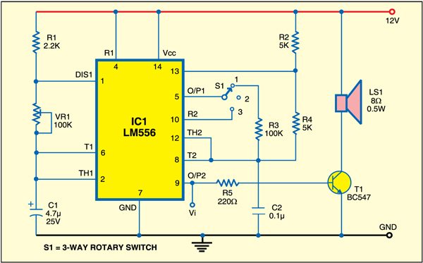
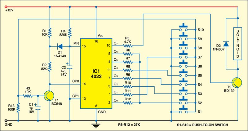
Here is a simple triple mode tone generator circuit that generates three different tones. You can use it as a call bell, burglar alarm or any other security alarm.

Triple Mode Tone Generator Circuit

Fig. 1: Triple mode tone generator circuit

Fig. 1 shows the circuit of the triple mode tone generator, while Fig. 2 shows its extension for an automobile horn. The circuit operates off a 12V battery. At the heart of the circuit is an LM556 dual timer IC having two separate LM555 timers built into it. The first timer is configured as an oscillator with a wide frequency range. The second timer is triggered by the output of the first timer. The circuit produces three sounds depending on the position of the rotary switch (S1). S1 is a single-pole, three-way switch.

Circuit operation

When switch S1 is at position 1, the output of the second timer at pin 9 produces a two-tone sound. When switch S1 is shifted to position 2, the output of the second timer at pin 9 produces a continuous tone. When switch S1 is shifted to position 3, the output of the second timer at pin 9 produces a tone burst. Since LM556 can sink only 200mA current, transistor T1 is used to amplify the output of the second timer and according to the tone, the speaker sounds.

Fig. 2: TDA 2030A amplifier for automobile horn

To get louder sound or make an automobile horn, connect the output of the second timer at pin 9, after disconnecting from resistor R5, to audio signal Vi (Fig. 2). The TDA 2030 amplifier provides a high output current with very low harmonic and cross-over distortion. A conventional thermal shut-down system is also included in it.

Assemble the two circuits on separate general purpose PCBs. The PCBs can be housed in a suitable enclosure.


The article was first published in July 2010 & has recently been updated.

The post Triple Mode Tone Generator appeared first on Electronics For You.

Leakage and Continuity Tester

$
0
0

Here is a simple, chargeable leakage and continuity tester that can be operated in two modes: normal mode and gain mode. The gain mode is especially useful for detecting small leakages in electrolytic capacitors or large resistors, which can’t be detected by ordinary continuity testers without amplification of the continuity current. The normal mode is used for continuity testing.

Continuity tester circuit

Fig. 1 shows the circuit of leakage and continuity tester. The use of a rechargeable battery (3.6V, 60mAh Ni-Cd) makes the instrument so compact and lightweight that it can be easily housed inside a glue-stick tube.

Circuit of leakage and continuity tester
Fig. 1: Circuit of leakage and continuity tester

Amplification of current continuity is achieved by using a transistor along with small base resistor R1 (1-kilo-ohm) such that its contribution in the closed circuit is small. Resistor R2 (100-ohm) in combination with signal diode D1 limits the charging current and direction.

The battery can be charged through the probes by connecting them to a 5V source. Use a transparent red LED (LED1) for easy detection of continuity.

Circuit operation

To check the leakage, flip S1 towards gain mode, clip the alligator clip to one terminal of the component under test, and touch the probe to the other terminal of the component. If LED1 glows, it indicates leakage.

Similarly, to check continuity, flip S1 towards normal mode. Clip the alligator clip to ground terminal of the circuit and touch the probe to the terminal that you want to check for continuity/shorting. If LED1 glows with high intensity, it indicates continuity.

Proposed arrangement for leakage and continuity tester
Fig. 2: Proposed arrangement for leakage and continuity tester

Continuity & testing

The proposed arrangement for this leakage and continuity tester is shown in Fig. 2. First, in the glue stick tube, make the necessary holes and a rectangular slot for the positive probe tip, LED1 and single-pole double-throw switch (SPDT) S1, respectively. Complete the entire wiring, except for the alligator clip and the switch, as shown in the schematic diagram.

Pull the wires for the alligator clip and the switch outside the glue-stick tube and then finish their soldering. Fasten the switch to the glue-stick tube. Similarly, fasten the positive gel-pen probe tip and then LED1 as shown in Fig. 2. The insulation card can be made from any thick paper or plastic (recommended) in round shape with a slot to pass wires through it. Now your leakage and continuity tester is ready to use.


The article was first published in June 2010 and has recently been updated.

The post Leakage and Continuity Tester appeared first on Electronics For You.

Viewing all 5950 articles
Browse latest View live