Quantcast
Channel: EFY Bureau – Electronics For You
Viewing all 5950 articles
Browse latest View live

IR Based Light Control

$
0
0

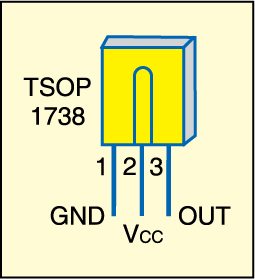
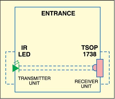
This IR based light control circuit turns on the lights at the portico, car parking or other areas when a motorbike or car enters through the gate to cross the sensing area. It can also be used as an electronic watchdog for your house, by activating an alarm simultaneously.

The system consists of a transmitter receiver pair along with a switching circuit. The transmitter and the receiver are mounted face to face on the opposite pillars of the gate such that the IR (infrared) beam produced by the transmitter falls directly on the IR sensor of the receiver. The system gets activated when someone passes through the gate to interrupt the IR beam falling on the sensor.

IR based light control circuit

IR based light control: Transmitter circuit

Transmitter

Fig. 1 shows the transmitter circuit. It consists of an infrared (IR) LED and an NE555 timer (IC3), which is wired as an astable multivibrator producing a frequency of around 38 kHz. The 38kHz infrared beam is transmitted through IR LED1.

IR based light control:  Receiver circuit
IR based light control: Receiver circuit

Receiver

Fig. 2 shows the receiver circuit. It consists of IR sensor TSOP1738, dual monostable multivibrator CD4538 (IC1) and a few discrete components.

When the IR beam falls on the sensor, its output pin 3 remains low and transistor T1 conducts to make pin 5 of IC1 high.

Fig. 3: Pin configuration of TSOP 1738

When anyone interrupts the IR beam falling on the sensor, its output pin 3 goes high to trigger IC1 (at pin 5) through transistor T1. As a result, output pin 7 of IC1 goes high for the preset time period. Transistor BC548 (T2) conducts to energise relay RL1 and LED1 is switched off. When the monostable time period is over, LED1 glows again.

The time period of IC1 can be increased or decreased by selecting a proper value for the capacitor connected between pins 1 and 2 of IC1. A three-position small rotary switch along with capacitors C3, C4 and C5 is used to select the time period of IC1.

Fig. 4: Mounting of transmitter and receiver units at the entrance gate

Diode 1N4001 (D1) acts as a freewheeling diode. The bulb (B1) to be switched on and off is connected between the pole of relay RL1 and neutral terminal of AC mains. It connects to the live terminal of AC mains supply via normally-opened (N/O) contacts of the relay when the relay energises.

Regulated 5V power supply for the transmitter and receiver units is derived from AC mains through step-down transformer X1, bridge rectifier (consisting of diodes D2 through D5) and regulator IC 7805 (IC2).

Construction & testing

Assemble the transmitter and receiver circuits on two separate general purpose PCBs and enclose in suitable cabinets. Fig. 3 shows the pin configuration of sensor TSOP1738. Mount the transmitter and receiver units on the opposite pillars of the gate as shown in Fig. 4.


The article was first published in June 2010 and has recently been updated.

The post IR Based Light Control appeared first on Electronics For You.


Greeniee – Optimize Energy Spends Through Data Driven Insights

$
0
0

In India, power utility bills are always a huge pandemonium, which includes the total usage for previous month and the amount to be paid by the customer for this usage. The consumer seldom knows the reason for paying this amount, and it becomes even more painful if the amount skyrockets randomly, it would take a toll on a normal man to decode the bill and understand the figures and causes. Apart from the usual suspects like AC or Geysers, a customer is hardly able to understand what caused the spike in bill. But,

  • What if consumers received alerts when their consumption is going out of control.
  • What if consumers received a detailed report of their energy bill – the amount they spent on lighting, the expenses on HVAC, the cost of running the Geyser, energy consumed by tv etc.
  • What if someone suggested means of reducing consumption and in turn bringing savings on energy bills.

This is exactly what happens at Greenturn Idea Factory (GIF). The customers are empowered with data driven insights, so that he or she can take an informed decision regarding their power consumption.

Greeniee -the Green Genie

The product Greeniee, is a smart energy assistant, which once installed at a consumer premise, can keep track of energy consumption at a granular level. The parameters recorded are sent over to the cloud for further analytics, where the patent-pending algorithm sieves through this data to detect appliance activity, thereby delivering a detailed report of the consumer’s energy expenses. Using state-of-the-art pattern recognition routines and ML-driven prediction mechanism, the algorithm separates out appliance activity from this overall energy data, thereby enabling a detailed energy usage report.
Users can track their energy consumption in the real-time on a smartphone app or web interface 24x7x365. “Greeniee is a single hardware that sits in the premise and watches over the overall consumption.”, says Sajil Peethambaran, Co-founder & Head of Technology, Greenturn Idea Factory.

What makes Greenie Intelligent

Greeniee is also smart enough to predict unauthorized usage, identify appliances that need maintenance, identify leakages in the circuit. It can also warn users if high energy appliances like Iron Boxes, geysers etc are left on by mistake. The automation module of Greeniee can also switch off these appliances automatically, if the consumer wants to enable that feature.

The stimulus for this invention

“It was exactly over a year ago that one of us got a current bill at home and had a shock of our life seeing the billed amount, which was more than twice the normal amount. The meter reader was unable to help saying that the values corresponded to the data shown in the meter. After ruling out usual suspects (Read AC, washing machine) we were still clueless as to what the reason was for the latest bill. On discussing this with friends and family we realised that surprisingly this problem is one that affected over 75% of the public, people getting high bills and having no clue whatsoever.”, says Sajil.

The design challenges

Developing a cost-effective solution for energy monitoring is a challenge by itself. Especially because a user brings home a hardware for a lifetime, adding more wanted value to the product is essential. The Greeniee hardware could also act as a communication gateway for interfacing other home automation products. “It took us nearly 6 months to deploy our first set of beta products in the field. The beta tests and subsequent refinement of solution – both hardware and cloud / mobile app took another 4 months. “, says Sajil

The masterminds

Greenturn was founded by a team of 4 technical graduates from Kerala. Greenturn Idea Factory is a startup from Cochin, Kerala that focuses on developing innovative products for the future. The product, Greeniee, has won accolades from the Kerala Startup Mission (KSUM) and the Kerala State Electricity Board (KSEB). In fact, KSEB has awarded an innovation grant for the project.

Greenturn Idea Factory operates out of Kinfra Hi Tech park, Kalamassery, in the outskirts of Cochin. The startup was incubated at Maker Village Cochin, a first-of-its-kind incubator for Hardware startups in India.

Kerala State Electricity Board had given Greeniee access to 50 homes across the state of Kerala to run trials. The field trials have been going on for the past 6 months, that has helped the team to fine tune features and offerings. GIF is planning for a commercial launch of the product Greeniee by January 2018.

The post Greeniee – Optimize Energy Spends Through Data Driven Insights appeared first on Electronics For You.

New eHealth Solution Powers Senior Home Care

$
0
0

Collaboration with large health insurer affordably improves independent living

GREENSBORO, N.C., Jan. 05, 2018 — Qorvo, a leading provider of innovative RF solutions that connect the world, is helping seniors live more independently in their homes with the help of a new eHealth system powered by the company’s chipsets for the Internet of Things (IoT). Health insurer CZ will provide the system to 3,000 elderly customers in the Netherlands, marking the first deployment of a senior smart home solution by a large health insurance company.

eHealth technologies with whole-home sensor systems present an opportunity for health insurers and consumers to reduce healthcare costs and enhance quality of life. According to Grand View Research, the global eHealth market is expected to reach $308 billion by 2022, and the transition of the healthcare industry into a digital healthcare system for management and analysis of patient health is expected to be the most vital driver of the market.1

The system that CZ will deploy consists of a non-intrusive set of motion and open/close sensors, and a gateway. It combines proven cloud algorithm expertise from Sensara with industry-leading Zigbee Green Power RF solutions from Qorvo. Zigbee Green Power is optimized for ultra-long coin-cell battery life sensors (10-year replacement) and provides secure, long-range and highly reliable wireless data transmission. These features are essential to the evolution of the smart home.

Menno Janssen, strategic program manager of CZ, said, “We believe that seniors using reliable eHealth systems will gain a wide range of benefits, enhancing their quality of life and enabling their families or caregivers to have peace of mind that they are safe and healthy.”

Cees Links, general manager of Qorvo’s Wireless Connectivity business unit, said, “The innovation that Qorvo delivers in its Zigbee Green Power RF solutions, combined with behavior analysis algorithms, helps elderly people live longer and more independently at home. We’re excited about our partnership with CZ, a large health insurance company, and commend them for being a frontrunner in deploying eHealth solutions to improve lives. The IoT lifestyle market is quickly growing, and Qorvo is proud to play a more significant part.”

Qorvo products that solve the IoT’s toughest RF challenges will be showcased during CES 2018 (#CES2018) in Las Vegas, Nevada, January 9-12, in booth #42531, Halls A-D of Sands Expo.


The post New eHealth Solution Powers Senior Home Care appeared first on Electronics For You.

New Scalable Image Sensor Platform for ADAS and Autonomous Driving

$
0
0

New platform offers industry’s highest resolution at 8.3MP combined with most advanced automotive system level features

Consumer Electronics Show (CES) – Venetian 3302 – LAS VEGAS, NV – 5 January, 2018 – ON Semiconductor, driving energy efficient innovations, today announced a scalable family of CMOS image sensors to address the spectrum of applications for Advanced Driver Assistance Systems (ADAS) and autonomous driving. ON Semiconductor’s newest sensor family offers car makers and tier one suppliers a choice of robust imaging devices based on a common platform and feature set. The sensors have resolutions scaling from 8.3 megapixels (MP) down to 1.2 MP with industry leading low-light performance from 4.2 µm pixels. Additional features include functional safety up to ASIL-C, high-dynamic range (HDR), an industry-first cybersecurity option, and second-generation wafer stacking technology that reduces package size. Individual products in this platform are currently under evaluation by many technology partners, including Mobileye and NVIDIA for use with its DRIVE AI computing platform for autonomous vehicles.

The AR0820AT, AR0220AT and AR0138AT form a scalable image sensor family which provides a range of resolutions suited to new-generation ADAS and autonomous driving systems. Automakers need different resolutions to address segmentation in their product lines, where specific safety features are standard, but additional cameras or higher resolution cameras enable more advanced safety and luxury capabilities as customer options.

As the industry moves from Level 2 systems for emergency autonomous braking, adaptive cruise control and lane change assistance towards fully autonomous driving, ON Semiconductor’s image sensors enable increasingly demanding ADAS and autonomous driving capabilities. The large 4.2 µm pixel delivers leadership performance in low-light scenarios such as night-time emergency braking for pedestrians and cyclists that is being added to safety tests defined by Euro NCAP. The family’s cybersecurity technology helps ensure reliable and secure operation when multiple cameras around the vehicle are connected to a centralized system where data and commands must travel by wires between the sensor and the processor.

For advanced imaging capabilities, software and algorithm testing is typically the longest task in the development program. With ON Semiconductor’s family of scalable image sensors, customers can start early development with one sensor to adapt their algorithms to the pixel performance and system features, and then extend to additional resolutions with further testing. This shortens project time-to-market and reduces overall development costs across a family of camera system implementations.

“As the number of image sensors on a vehicle increases, having a scalable platform with common core features and pixel architecture becomes even more important for automakers to deliver new safety and self-driving features to market quickly and efficiently,” said Ross Jatou, vice president and general manager of the Automotive Solution Division at ON Semiconductor. “Our deep engagement with customers and the advanced features of our new image sensor family enable them to bridge development efforts across ADAS and autonomous driving programs.”

ON Semiconductor will be demonstrating its new family of scalable image sensors, plus a wide range of other leading edge semiconductor-based solutions for automotive and other sectors at The Sands Convention Center/Venetian (Murano 3302) during CES 2018, January 9-12 in Las Vegas. The company’s imaging experts will be available all week to answer questions regarding solutions for automotive image sensor applications.


The post New Scalable Image Sensor Platform for ADAS and Autonomous Driving appeared first on Electronics For You.

FPGAs in Data Centres: Opportunities and Challenges (Part 2 of 2)

$
0
0

Cont. from : FPGAs in Data Centres Part 1

Catapult cloud field-programmable gate array (FPGA) architecture accelerates both cloud services (such as search engine) and the Azure cloud platform; Azure is an open, flexible, enterprise-grade cloud computing platform. The reconfigurable Catapult fabric is embedded into each half-rack of 48 servers in the form of a small board with a medium-sized FPGA and local dynamic random-access memory (DRAM) attached to each server. FPGAs used in Catapult servers are central to delivering better Bing results. These can quickly score, filter, rank and measure the relevancy of text and image queries on Bing.

Catapult v2 design is more flexible in circumventing traditional data centre structures for machine learning and expands the role of FPGAs as accelerators. It expands the availability of FPGAs, allowing them to be hooked up to a larger number of computing resources. FPGAs are connected to DRAM, central processing unit (CPU) and network switches. These can accelerate local applications, or act as a processing resource in large-scale, deep-learning models. Much like with Bing, FPGAs can be involved in scoring results and training deep-learning models.

Deep learning

Fig. 16: Deep learning

Catapult v2 design can be used for cloud-based image recognition, natural language processing and other tasks typically associated with machine learning. It could also provide a blueprint for using FPGAs in machine learning installations. Many machine learning models are driven by graphical processing units (GPUs), but the role of FPGAs is less clear. FPGAs can quickly deliver deep-learning results, but consume too much power if not programmed correctly. These can be reprogrammed to execute specific tasks, but that also makes them one-dimensional. In comparison, GPUs are more flexible and capable of handling several calculations.

Catapult server specification

Project Catapult employs an elastic architecture that links FPGAs together in a 6×8 ring network that provides 20Gbps of peak bidirectional bandwidth at sub-microsecond latency. It allows FPGAs to share data directly without having to go back through the host servers. It can reprogram the Catapult fabric to adapt to new ranking algorithms without the time and cost of developing custom ASICs or the disruption of having to pull servers from production to install new ASICs—a primary consideration when operating cloud-scale data centres.

Drivers for deep learning

Fig. 17: Drivers for deep learning

Microsoft is putting FPGAs on PCI Express networking cards in every new server deployed in its data centres. FPGAs handle compression, encryption, packet inspection and other rapidly changing tasks for data centre networks that in six years have jumped from Gbps to 50Gbps data rates. In comparison, GPUs are typically more power consuming and more difficult to program.

Power9 processors use Nvidia’s NVLink to connect to chips like Pascal as well as IBM’s own CAPI to link to FPGAs from Xilinx. Separately, ARM will use its Coherent Hub Interface to link to Xilinx FPGAs and other accelerators. The x86 giant is already showing packages that contain Xeon server and Altera FPGA die. It aims to put both the chips on a single die as early as next year. Both CPUs and FPGAs require a lot of power. Putting the two in one socket will limit performance to the thermal envelope of the single chip.

Altera vs PCI

Fig. 18: Altera vs PCI

Microsoft is using Altera FPGAs both in its networking cards and as accelerators for its Bing search. China server vendor Inspur is trying to ride the GPU train with a server packing 16 graphics processors. The server uses a message passing interface the company created for the Caffe deep learning framework developed at U.C. Berkeley for use with GPU accelerators. FPGAs accelerate the ranking of search terms—a new partition of the overall search job.

A special embedded core makes the FPGA more programmable. China’s Baidu has developed an FPGA board accelerating at least ten low-level tasks. The PCIe 2.0 card uses a Xilinx K7 480t with 4GB memory.

Catapult uses a network of directly linked FPGAs

Fig. 19: Catapult uses a network of directly linked FPGAs

Speedster 22i FPGAs built on Intel’s advanced 22nm process technology implement all of interface functions as hardened IP. This results in lower power consumption, reduced programmable logic fabric, faster clock rates, and simpler design since the interface IP is already timing-closed.

Achronix Accelerator-6D board is said to offer the highest memory bandwidth for an FPGA-based PCIe form factor board. This PCIe add-in card is well suited for high-speed data centre acceleration applications. The Accelerator-6D packs a Speedster22i HD1000 FPGA with 700,000 lookup tables, which connects to six independent memory controllers to allow up to 192GB of memory and 690Gbps of total memory bandwidth. Accelerator-6D board comes with a power supply, one-year licence for Achronix ACE design tools, and multiple system-level reference designs for Ethernet, DDR3 and PCIe operation.

The post FPGAs in Data Centres: Opportunities and Challenges (Part 2 of 2) appeared first on Electronics For You.

How E-Paper Displays Different From That of Normal Displays?

R-REF01-HB Universal Half-Bridge Reference Design

$
0
0

RECOM opens new doors with its universal half-bridge reference design which is a platform design that can be used to compare the real-life performance of various high power IGBT, 1st/2nd generation SiC, GaN, MOSFET and Cascode switching technologies. As the gate driver and PCB layout is the same for every transistor type, users will be able to compare and contrast their real-life switching performance and make informed choices about the right technology for their application.

The reference design consists of a half-bridge layout with a fully isolated driver stage using isolated power supplies for both the low-side and the high-side switching transistors. Included in the package are four sets of different DC/DC converters which generate the appropriate isolated driver voltages for the different transistor types. The user can thus select which TO247 or TO247-4L (Kelvin connection) packaged switching transistors they wish to evaluate from the supplier of their choice, fit the appropriate DC/DC converter to match and then rapidly prototype and test their application. The reference design is a basic building block that can be used to evaluate forward, flyback, buck and boost topologies and by combining two or more units it can be used to evaluate full-bridge and 3-phase bridge circuits. The PCB is optimized for high-speed switching up to 1000V at up to 10A gate drive current. The signal ground is galvanically isolated from the power ground and on-board BNC sockets are fitted for high speed connections to the external TTL signal generators. As the high-side and low-side control are separate, the reference design can also be used to implement asymmetric duty cycle, active clamp and phase shifted full-bridge topologies.

The post R-REF01-HB Universal Half-Bridge Reference Design appeared first on Electronics For You.

Cost-Effective Thermal Cameras to Aid Incident Response and Intrusion Detection

$
0
0

Bangalore, 05 January, 2018: In launching the first thermal cameras in its P-line – Axis Communications is bringing the benefits of thermal imaging to a broader range of customers and environments than ever before. The cost-effective cameras deliver thermal imaging capabilities to small and mid-size systems with budget limitations – such as schools, care environments and independent retailers– allowing for intrusion detection and incident identification, without compromising individuals’ identities.

Thermal technology is renowned for ensuring reliable detection with a low rate of false alarms, but until now the cost of high-quality thermal imaging has been beyond the reach of organizations with limited budgets. The new AXIS P1280-E Thermal Network Camera is an indoor/outdoor camera with a flexible form factor that allows the thermal sensor unit to be placed in locations with limited space and it comes with a wide range of mounting accessories for both wall, ceiling or recessed installations. AXIS P1290 Thermal Network Camera is an indoor camera protected in a dome casing for discretion.

Ideally, they can be used as a cost-effective detector with visual confirmation for safety of both people and property in numerous environments. The cameras have built-in analytics, such as AXIS Video Motion Detection that can send an alert when it detects motion from moving objects within a predefined area. The cameras also support AXIS Camera Application Platform, which is compatible with a broad range of third-party applications.

Martina Lundh, Global Product Manager at Axis Communications explains the benefits of thermal imaging: “In environments where the privacy of individuals is paramount – for example schools and care homes – thermal imaging detects incidents without revealing personal details of the people in the image. Together with analytics these new cameras can trigger alerts or alarms in response to patient or resident falls, allowing staff to take immediate action.”

“In care environments, staff can observe patients and residents remotely, so that staff can work more efficiently, and patients and residents can rest undisturbed. In the same way, it is possible to use thermal imaging to observe student movements through a school, without having staff physically present in every room or hallway and without invading the student’s privacy. In addition, cameras can be used inside and outside schools to identify unauthorized access before, during or after school hours.”

The post Cost-Effective Thermal Cameras to Aid Incident Response and Intrusion Detection appeared first on Electronics For You.


Add-on USB Power Circuit For UPS

$
0
0

Most computer UPS have only 230V output and no USB output. Presented here is a USB power circuit that gives 5V USB output using the 12V, 7Ah UPS battery fitted inside a UPS. With this circuit you can power USB gadgets directly from a UPS without turning on the PC. This circuit can also be used to power development boards like Arduino and Raspberry Pi.

Circuit and working

As shown in Fig. 1, the circuit is built around switch-mode regulator LM2576-5V (IC1). The LM2576 series offers a high-efficiency replacement for popular three-terminal linear regulators. It substantially reduces the size of the heat-sink; in some cases, no heat-sink is required. It provides all the active functions of a step-down (buck) switching regulator, capable of driving up to 3A load with excellent line and load regulation. The 5V version of LM2576 (LM2576-5V) is used in this circuit.

Circuit diagram of add-on USB power circuit for UPS

Fig. 1: Circuit diagram of add-on USB power circuit for UPS

The 12V battery is connected to CON1. IC1, along with inductor L1 and diode D1, steps down and converts the 12V input into 5V output. Capacitor C2 reduces ripples in the output. Feedback pin 4 of IC1 is directly connected to the output at C2.

IC1 can be turned on/off by an external control signal or else it can be turned on permanently by grounding pin 5 of IC1 through switch S1. When S1 is in position A, IC1 can be controlled by connecting an external control signal at CON3. When S1 is in position B, IC1 is switched on permanently. LED1 indicates whether IC1 is on or off. This circuit can be used to power gadgets digitally.

Construction and testing

A PCB layout for the add-on USB power circuit for a UPS is shown in Fig. 2 and its components layout in Fig. 3. Assemble the circuit on the PCB and place it at a suitable location inside the UPS.

PCB layout of add-on USB power circuit for UPS

Fig. 2: PCB layout of add-on USB power circuit for UPS
component layout

Fig. 3: Components layout for the PCB

Download PCB and component layout PDFs: click here

Use suitable heat-sink for IC1. Inductor L1 must have a minimum current rating of 1A. Capacitor C2 should have low equivalent series resistance (ESR) for better performance. Any voltage from 7-40V can be used for the circuit.

parts list

If the external control signal is open-collector type, a suitable pull-up resistor must be used on pin 5 of IC1. Do not leave this pin float. To maintain stability, capacitor C1 leads must be kept short and placed near IC1.


The post Add-on USB Power Circuit For UPS appeared first on Electronics For You.

Advanced Battery Management System Enables a Safer, Smarter Car of the Future

$
0
0

Maxim’s unique BMS technology, including MAX17843, has the industry’s only single-chip solution to achieve ASIL D compliance

San Jose, CA and Las Vegas, NV—January 9, 2018—Automotive OEMs can enhance the safety of their lithium-ion battery packs with robust communications, comprehensive diagnostics, and lower system costs with the MAX17843 12-channel, high-voltage smart sensor data-acquisition device from Maxim Integrated Products, Inc.

Electric vehicles (EVs), hybrid EVs, and plug-in hybrids rely on large lithium-ion battery packs filled with hundreds or even thousands of individual battery cells. With industry experts predicting that 25% of cars sold by 2025 will have electric engines, automotive OEMs and Tier 1s need an intelligent battery management system to enable safe, low cost solutions with robust communications.

Maxim is enabling a safer, smarter car of the future with the MAX17843 battery management system (BMS). MAX17843 meets the highest safety standards, adhering to ISO 26262 and ASIL D requirements (also applicable for ASIL C). Its differential universal asynchronous receiver/transmitter (UART) using capacitive isolation reduces bill of materials (BOM) costs and failure in time (FIT) rates. With this, designers can save up to 90% of their isolation BOM cost. The UART, with ultimate flexibility, enables robust communications in noisy environments. Using Maxim’s unique proprietary daisy-chain architecture and successive-approximation-register (SAR) analog-to-digital converter (ADC), the MAX17843 captures fast, accurate voltage measurements and delivers high EMC performance. It is applicable for a variety of automotive and EV powertrain applications.

Key Advantages

Safety: ISO 26262 and ASIL D certification, as well as TUV certification in design and management process; meets various BCI requirements; comprehensive diagnostics

Low System Cost: Internal cell balancing and UART reduces BOM costs compared to competitive solutions; only IC to allow capacitive or transformer isolation

Robust Communications: Reliable distributive and centralized CMC architecture with UART; Supports 100m daisy-chain segments and high noise immunity; Supports emission, ESD, and hot plug


The post Advanced Battery Management System Enables a Safer, Smarter Car of the Future appeared first on Electronics For You.

Artificial Intelligence Is a Game Changer for Personal Devices

$
0
0

AI Will Drive the Most Compelling User Experiences at Home and in the Workplace

New Delhi, India, 9th January, 2018 — Emotion artificial intelligence (AI) systems are becoming so sophisticated that Gartner, Inc. predicts that by 2022, personal devices will know more about an individual’s emotional state than his or her own family. AI is generating multiple disruptive forces that are reshaping the way we interact with personal technologies.

“Emotion AI systems and affective computing are allowing everyday objects to detect, analyze, process and respond to people’s emotional states and moods to provide better context and a more personalized experience,” said Roberta Cozza, research director at Gartner. “To remain relevant, technology vendors must integrate AI into every aspect of their devices, or face marginalization.”

The current wave of emotion AI systems is being driven by the proliferation of virtual personal assistants (VPAs) and other AI-based technology for conversational systems. As a second wave emerges, AI technology will add value to more and more customer experience scenarios, including educational software, video games, diagnostic software, athletic and health performance, and the autonomous car.

“Prototypes and commercial products already exist and adding emotional context by analyzing data points from facial expressions, voice intonation and behavioral patterns will significantly enhance the user experience,” said Ms. Cozza. “Beyond smartphones and connected home devices, wearables and connected vehicles will collect, analyze and process users’ emotional data via computer vision, audio or sensors capturing behavioral data to adapt or respond to a user’s wants and needs.”

Other personal device predictions from Gartner include:

By 2021, 10 percent of wearable users will have changed lifestyles, and thereby extend their life spans by an average of six months.

As AI emotion systems evolve there is huge potential for specialized devices, such as medical wristbands, which can anticipate life-threatening conditions and facilitate an early response system. At the same time special apps are also being developed for diagnostic and therapy services that will help to recognize conditions such as depression or help children with autism.

“Even a basic wearable device could have a positive impact on the wearer’s health,” said Annette Zimmermann, research vice president at Gartner. “We are seeing growing numbers of users actively changing their behavior for the better with the adoption of a wearable device. Not only can this have beneficial influence on the amount of exercise they do but there is evidence that one or two out of 10 smart watch and fitness band users discover a condition such as sleep apnea or cardiac arrhythmia through wearing the device.”

By 2020, 60 percent of personal technology device vendors will use third-party AI cloud services to enhance functionality and services.

Cloud-based AI technologies are driving compelling user experiences on a variety of connected devices. Cloud offerings from the big tech players, such as Google, Microsoft, Amazon, Tencent, Baidu and IBM, are starting to proliferate due to their attractive cost model, easy-to-use integration and potential to create complex services. A major catalyst for device vendors to use cloud AI services is the increased usage of VPAs and natural-language technologies, while the adoption of VPA-based, screenless devices such as Amazon Echo and Google Home is also on the rise, further increasing usage of cloud AI services.

“We are starting to see adoption of these services from high-profile vendors that are using them to widen their reach,” said Anthony Mullen, research director at Gartner. “Fitbit uses Alexa Skills to make user stats and functionality available through VPA speakers just as Netflix uses Actions for Google Assistant to voice control its service. Ultimately, vendors will compete on the best user experience and the smartness of their products, not the technology behind it.”

Through 2022, security technology combining machine learning, biometrics and user behavior will reduce passwords to account for less than 10 percent of all digital authentications.

Password-based simple authentication is becoming less and less effective for personal devices. Even today’s popular biometric technology — fingerprint authentication — is only around 75 percent successful due to contaminants such as dirt and sweat.


The post Artificial Intelligence Is a Game Changer for Personal Devices appeared first on Electronics For You.

Ruggedise the Hardware: Increase Its Life

$
0
0

McLaren-Honda, manufacturer of premium electric racing cars, recently started using silicon-carbide (SiC) power devices in inverters and on-board chargers, which increased their efficiency by 1.7 per cent while also reducing the cooling system size by 30 per cent. Thus, a change in the power component not only made their inverter compact but also rugged for use in electric cars. Similarly, gallium-nitride (GaN) power devices increase the reliability of low-power products.

“Both SiC and GaN-based power-conversion devices are creating a difference and making the product rugged,” says Niranjan G., general manager (business development & technical marketing), ROHM Semiconductor.

Ruggedising electronic hardware: external and internal

A hardware system needs to be electrically as well as physically rugged so that it can withstand harsh environmental conditions, electrical faults, component failures, mechanical faults, etc.

SiC and GaN market analysis (Image courtesy: www.pntpower.com)

Fig. 1: SiC and GaN market analysis (Image courtesy: www.pntpower.com)

For instance, for LED luminaires, designers select LED devices based on the application requirements of lumens, life-time, intensity and colour temperature. Optical component selection is also based on the application. Power supply is designed keeping in mind the desired current, voltage, power input, total harmonic distortion (THD) and power factor. Mechanical part is based on the thermal dissipation of the luminaire as a whole.

Besides, designers follow various manufacturing standards that are important from ruggedness point of view. LM79 standard is followed for LED luminaire performance test, and LM80 for LED evaluation. IPXX standards are followed for protection of LED luminaires and power supply from environmental conditions such as air, water, dust, physical contact and accidental contacts. IEC, EC, UL and BEE standards pertain to the quality of a hardware product.

The hardware includes the PCB and components on the PCB. Be it an analogue solution, power solution, sensing solution or mobile solution, hardware must be well-built and rugged.

Analogue and power solutions

There have been industrial upgrades in the quality of the PCB, power components and their hardware applications at electrical or physical level.

PCB and improved substrate

The PCB is an essential element of a hardware as it provides the base or the platform to the circuitry. The PCB material is chosen based on the type of application. For instance, as a small power supply with less input and output current will dissipate very less heat, it can be built on an FR4-based PCB, which costs very less.

Hrishikesh Kamat, CEO of Shalaka Connected Devices, says, “Multilayer boards have been prepped up to 256 layers by tech giants.”

As electronic devices shrink, PCBs are becoming smaller and multilayer to support connectivity with several components at a time. Complexity of the circuitry is increasing and the technology is getting sophisticated. The average thickness of the PCB ranges between 0.5mm and 0.7mm, which, technology experts believe, will decrease further to 0.4mm or less. This will open up new possibilities in the wearables domain.

Traditionally, PCB prepregs have been fibreglass or epoxy, but now substrates are available in several other materials too, such as resin-coated copper, resin-coated film and liquid-crystal film. These prepregs maintain the signal integrity of a circuit and high-end processing at low costs.

Thus, improved PCB substrate and reduced PCB thickness ensure high signal integrity and low output losses, resulting in a reliable and rugged hardware.

Smaller, stronger, faster components

Silicon carbide is becoming the industry-leading technology in power conversion, contributing to the eco-friendly environment. ‘Trench-structure’ design contributes to the long-term reliability of components. Nowadays, these trench-structure MOS devices are acting as alternatives to relays in automobiles (especially electric vehicles) due to their high current handling capability. Their other field applications include industrial automation equipment, solar power inverters, digital power supplies of large-scale servers in data centres and home appliances such as air-conditioners.

Ruggedising Electronic Hardware

For low-power and medium-power applications, trench-structure devices provide many advantages:

1. Structural change lowers the drain-to-source resistance (RDS ON) and thus heat dissipation, making the end product efficient
2. Breakdown voltage and switching frequencies of trench-structure MOSFETs and other components using SiC are generally higher than conventional FETs
3. Low on-resistance, high breakdown voltage, high current and high frequencies enable a compact and efficient cooling system
4. The compact size of the component helps in reducing the size and the cost of the PCB
“Thus, silicon carbide reduces the overall system costs and helps in energy conservation by making efficient end-products,” says Niranjan.

Trench power MOS in SiC device (Image courtesy: patentimages.storage.googleapis.com)

Fig. 2: Trench power MOS in SiC device (Image courtesy: patentimages.storage.googleapis.com)

Chip resistor—no more laser cuts for accurate value

Niranjan says, “Thermo-mechanical stress causes resistor failure, so manufacturers are coming up with a techno-logy that allows solder application on the lateral side of the resistor chip.”

Chip resistors’ solder area on their lateral side assists them to sit well on copper pads, avoiding short-circuit and open-circuit faults and breakage due to thermal and mechanical stresses. This helps the resistors to remain cracks-free for a long term.

As far as the manufacturing of chip resistors is concerned, earlier laser cuts were carried out to adjust the resistor value. With that method, usually, the resistor value did not exactly match the customer requirement. Now the practice of laser cuts in resistors has been discontinued, which allows resistor values according to specifications.

The post Ruggedise the Hardware: Increase Its Life appeared first on Electronics For You.

ADI 72V Hybrid Step-Down DC/DC Controller Reduces Solution Size by 50% Compared to Traditional Architectures

$
0
0

Bangalore – January 10, 2018 – Analog Devices, Inc. has announced the Power by Linear LTC7821, an industry first hybrid step-down synchronous controller that merges a switched capacitor circuit with a synchronous step-down controller, enabling up to a 50% reduction in DC/DC converter solution size compared to traditional step-down solutions. This improvement is enabled by a 3 times higher switching frequency without compromising efficiency. Alternatively, when operating at the same frequency, a LTC7821-based solution can provide up to 3% higher efficiency. Other benefits include low EMI and reduced MOSFET stress due to a soft-switched front end, ideal for next generation non-isolated intermediate bus applications in power distribution, datacom and telecom as well as emerging 48V automotive systems.

The LTC7821 operates over a 10V to 72V (80V abs max) input voltage range and can produce an output voltage from 0.9V to 33.5V with currents in multiple 10s of amps, depending on the choice of external components. In a typical 48V to 12V/20A application, an efficiency of 97% is attainable with the LTC7821 switching at 500kHz. The same efficiency can only be achieved in a traditional synchronous step-down converter by switching at one-third the operating frequency, resulting in the use of much larger magnetics and output filter components. External MOSFETs switch at a fixed frequency programmable from 200kHz to 1.5MHz. The LTC7821’s powerful 1 Ohm N-channel MOSFET gate drivers maximize efficiency and can drive multiple MOSFETs in parallel for higher power applications. Due to its current mode control architecture, multiple LTC7821s can be operated in a parallel, multiphase configuration with excellent current sharing to enable much higher power applications.

The LTC7821 implements many proprietary protection features for robust performance in a wide range of applications. An LTC7821-based design eliminates the inrush current typically associated with switched capacitor circuits by pre-balancing the capacitors during start-up. The LTC7821 also monitors system voltage, current and temperature for faults, and uses a sense resistor for overcurrent protection. It stops switching and pulls the /FAULT pin low when a fault condition occurs. An onboard timer can be set for appropriate restart/retry times. The EXTVCC pin enables the LTC7821 to be powered from the lower voltage output of the converter or other available source up to 40V, reducing power dissipation and improving efficiency.

The LTC7821 is available in a 5mm x 5mm QFN-32 package. Extended and industrial temperature versions are available from –40 to 125°C. For more information, visit www.linear.com/product/LTC7821.

LTC7821 Product Features

  • Wide VIN Range: 10V to 72V, 80V Abs Max
  • VOUT Range: 0.9V to 33.5V
  • Up to 50% Reduction in Solution Size
  • Soft Switching for Low EMI and Reduced MOSFET Stress
  • Up to 97% Efficiency at 500kHz
  • PLL Fixed Frequency from 200kHz to 1.5MHz
  • Clock Output for Multiphase Operation
  • Powerful Quad N-Channel MOSFET Gate Drivers
  • Input Current Sensing & Overcurrent Protection
  • Short-Circuit Protection with Programmable Timer & Retry

The post ADI 72V Hybrid Step-Down DC/DC Controller Reduces Solution Size by 50% Compared to Traditional Architectures appeared first on Electronics For You.

India is More a Hub for Engineering Design Service Today Than Earlier

$
0
0

Element14 recently inaugurated their biggest office in Bengaluru, India, a behemoth over 33,000 sqft big, with support for Indian as well as global services. EFY caught up with element14 executives, Graham McBeth, Ralf Buehler, and Uma Pingali as they took us on a guided tour along a panoramic view of the new space.


Ralf Buehler
Ralf Buehler

Q. Can you please tell us a bit about element14 and your Avnet acquisition last year?

A. Graham: element14 is a large company, we are owned by Avnet since last one year. We have spread in Europe, North America, Asia pacific, this is our element14 component business. We have another company which sell more electrical wholesale products, they have a business around 210 million. The main element14 component business represent in India or in Asia contains with in the 117 million of APAC. We have 2 million customers, and we have a large customer care. We get about 30 thousand new customers in to the business every month. Lot of customers coming and finding us and buying new things, which is exciting for us. We have 8 warehouses, we still believe in having warehousing course to the customer, we have a 3 PL warehouse in Bangalore or in India. We have invested quite a lot in the last 6 months in inventory. We have an amazing element14 community, we have about 500 thousand people now in our community. Electronic engineers speak to each other about product solutions, we run lots of road tests, events, webinars etc. Another complement is Avnet recently bought a company called AXIOM, which is world’s second biggest community, they have 300 thousand members. So Avnet now the largest communities in the world, and we collaborating together with element14. We have taken advantage of each other’s skills, and comparing with shared experiences.

Graham McBeth
Graham McBeth

Q. What are the main focus areas for element14 moving forwards?

A. Ralf: Especially in the electronic industry, industry is changing quite a bit from traditional OEM’s types with product scape develop, more in to a network environmental development. There are lot of IOT innovations happening in non-traditional companies. So we really focused on 4 segments across the whole value chain, we are really focusing on education, because we try to help people to get in to engineering and also help them, create business out of the education. We support research and design, idea creation and realizing these ideas. Typically lots of technology information is required, lots of fast delivery of small quantities initially to get things started early. We are trying to help the idea getting into production. We offer not just wide range of components, but all types of tests and measurement equipment, anything that would speed up your development cycle time. Single board computer for that matter is a platform, wherein you don’t have to develop from the ground up for yourself. End of all of that, we trying to make your production seamless by giving you the components, helping you to maintain your machines or in the worst case, when products get obsolete, help you to re-engineer your products again.

Q. Please talk to us about the boards business, are Customized boards making a comeback?

A. Graham: For us, boards are very attractive business with limited competition. We do a 100 million dollars of business in boards. So we are trying to differentiate customized boards more and more now. We are looking at kitting options for customers, providing better tools for coding large belt of material etc. We want to continue to focus on being a differentiated distributor in the market place.

Q. I think BBC has micro-bit, right? Micro bit was started off with very amazing idea, to get children in to programming, Now it’s coming to India. Talk to us about that.

A. Ralf: Yes it is very exclusive, we manufacture micro-bit, and it is coming to India now. When we talk about customization, the micro bit is not really the product we would customize, because it has got core functionality, which is trying to get children or students into programming. As a next step, you could say a Raspberry Pi coming from micro bit, there we can do customization. If you need even more power, again we have a BB board, there you can do customization. In IoT space, around the world, lot of software element of app building and cloud based services, people don’t necessary want to build hardware. The hardware platform is what they can utilize to create their products, that’s we are heavily focused on open source hardware, is really we considered the next big battle ground, because the more you can proliferate the board in to the market, the eco system will going to be better in terms of developing software by developers, more software code available easier to get in to the market. That way we are trying to help through manufacturing and selling it.

The post India is More a Hub for Engineering Design Service Today Than Earlier appeared first on Electronics For You.

Wi-Fi Solutions Enable Small Form Factors, Reduce Cost of Network Maintenance

$
0
0

GREENSBORO, NC, – January 8, 2018 – Qorvo, a leading provider of innovative RF solutions that connect the world, is enabling the expansion of distributed Wi-Fi solutions in the home through a portfolio of 802.11ax products that improves Wi-Fi coverage, enables smaller devices and reduces costs. These products include Wi-Fi front end modules, Wi-Fi BAW 2.4GHz bandedge and LTE coexistence filters, and Wi-Fi integrated front end modules (iFEMs).

“In the last year, we have seen a flood of new distributed Wi-Fi mesh network products released in the marketplace,” said Christian Kim, senior analyst, IoT and connectivity, for IHS Markit, a global business information provider. “With the addition of smart home devices and the increasing home use of streaming services, such as Netflix or Spotify, we expect to see continued introduction of new distributed Wi-Fi mesh systems in 2018.” 1

Distributed Wi-Fi networks, also known as Wi-Fi mesh, use multiple routers to spread Wi-Fi signals throughout the home. Qorvo maximizes the output power of in-home Wi-Fi signals while simultaneously optimizing their efficiency and lowering power consumption. The company’s Wi-Fi modules enable consumers to fully utilize the frequency band, whereas competitive products with sub-par filters have trouble accessing the full spectrum.

As a result, Qorvo technology delivers expanded coverage and reduced energy costs for consumers, while service providers and manufacturers benefit from improved customer satisfaction and fewer service calls and truck rolls.

Cees Links, general manager of Qorvo’s Wireless Connectivity business unit, said, “The notion of ‘power’ can be confusing, but Qorvo’s innovation labs have figured out how to maximize the output power of Wi-Fi signals throughout the home, while optimizing efficiency to lower power consumption. With Qorvo’s advanced RF technology, equipment makers can create distributed Wi-Fi networks that use unobtrusive end devices throughout the home, eliminate dead spots, and scale to more applications and users. Qorvo eliminates Wi-Fi problems before they emerge.”


The post Wi-Fi Solutions Enable Small Form Factors, Reduce Cost of Network Maintenance appeared first on Electronics For You.


Turn Your Android Phone into Home Security Camera

$
0
0

For those who do not want to invest in separate surveillance cameras and go through the hassle of installation, configuring a spare Android smartphone to serve the purpose is the best option. You can use your smartphone to invigilate your premises, alert you during any unexpected motion, or answer your door and communicate with whoever is on the other end. The best part is that home security applications are free and supported by almost all operating systems and devices, while the setup requires hardware you already have!

What you need

  • Smartphone (or tablet) that you will use as the security camera
  • Device (another smartphone, computer or tablet) that you will use to monitor the stream feeds and receive notifications
  • Suitable mobile application of your choice
  • Power source to keep the phone being used as security camera charged
  • Wi-Fi network at home

Which application to use?

From an exhaustive list of available security apps for Android, you can select one that suits your requirements:

Manything.

Besides common features of live streaming, motion detection, alert notification, night vision and two-way interaction, Manything allows users to customise its functionality.

Alfred.

Alfred application setup requires a valid Gmail account of the user. You can add multiple camera devices to your account—each device will require the application to be installed separately, but logged in with the same Gmail account.

AtHome.

Two separate apps are required to complete the whole setup—the app to be downloaded on the phone for recording is called AtHome Home Security, while another app used to view live streaming from the monitoring device is called AtHome Video Streamer—Monitor. The two devices can be connected with the help of a unique connection ID (CID) or a QR code.

IP Webcam.

IP Webcam is quite popular. In addition to regular features, it enables sensor data acquisition and analytics in its advanced applications.

What you have to do

1. Download the selected application on your spare smartphone (or tablet) and create a login account
2. Select the option to add a camera. Once done, personalise security camera settings. For example, you can name your device, choose to keep audio ‘on,’ select notification settings and so on
3. Once you have fixed the camera screen, leave it ‘on’ for recording
4. Place the camera-phone in the area you want to cover, ensuring that the area has a power socket to charge the device and good Wi-Fi coverage.

After setting up the camera device, prepare your monitoring device—your regular phone or your computer—as follows:

1. Download an appropriate application to this device. It may be the same application or a different interface from the same vendor, depending on your original selection
2. Log in with the account used for the other device. Additional steps for establishing a network between the devices may or may not be required
3. Now you will be able to view the streams on your mobile or computer, whichever you have used to setup the monitoring system.

Tips

Generally, rear cameras have better resolution and quality. So it is advisable to use a rear camera as the main recording camera.

Fix the camera such that it covers a bigger area. You may choose to use external lenses as well to increase the field of view.

For any application related problem, restart the application or check your network connection.


The post Turn Your Android Phone into Home Security Camera appeared first on Electronics For You.

Why are There No New Mobile Operating Systems?

$
0
0

In this video, the presenter will try to answer the most common question i.e. “Why are there no new mobile operating system?” at least in 2017-2018. What a technology firm or a developer requires to build a new Mobile OS? And, what new Mobile OS should consist of to beat the two most popular mobile OS “Android” and “iOS”?

Courtesy: TechAltar


The post Why are There No New Mobile Operating Systems? appeared first on Electronics For You.

Supercapacitors: Fundamentals and Applications

$
0
0

Energy crisis and environmental pollution have triggered the development of clean and renewable energy storage systems. Supercapacitors also called ultra-capacitors or Electrical Double Layer Capacitor (EDLC), provide very high capacitance in a small package. It stores electric energy in the form of the electric field between two conducting plates and can complete hundreds of thousands more charge-discharge cycle than batteries because they do not experience wear and tear associated with the chemical reaction. Due to this reason and its increased use in electric drives, UPS, active filters, traction and automotive drives has grabbed the attention to know the peculiarity of it.

Structure of Supercapacitor

Before we move on to the working of Supercapacitors, let us first understand the structure of a supercapacitor.

Supercapacitor cross-section

Figure 1. Supercapacitor cross-section

It does not consist of a dielectric material like ceramic capacitors or electrolyte capacitors do have. As shown in figure 1, supercapacitors consist of two porous electrodes, electrolyte, a separator and current collectors. Let us look at each of these.

Current collector:

Current collectors are made up of metal foil generally of aluminum as it is cheaper than titanium, platinum etc. They are coated with the electrode material.

Electrodes:

The capacitance value is proportional to the surface area of the electrode. Generally, as an electrode material, highly porous powdered coated active carbon material or carbon nanotubes are used. The porous nature of the material allows many more charge carriers (ions or radicals from electrolyte) to be stored in given volume. This increases the capacitance value of supercapacitors. The electrodes are coated on a current collector and immersed in an electrolyte.

Electrolyte:

The electrolyte is the key factor in determining the internal resistance (ESR). The electrolyte solution shall be either aqueous or non-aqueous in nature. The non-aqueous electrolytes are mostly preferred as they provide high terminal voltage V. Non-aqueous solution consists of conductive salts dissolved in solvents. Acetonitrile or propylene carbonate as solvents preferred mostly. Tetraalkylammonium or lithium ions can be used as solutes.

Separator:

The separator is between electrodes and it is made up of material that is transparent to ions but is an insulator for direct contact between porous electrodes to avoid short circuit.

The structure of supercapacitor is unique and hence it differs from conventional batteries and capacitors. Use of activated carbon increases surface area and hence increase in capacitance value. Electrolyte with low internal resistance increases power density. These both together brings ability in supercapacitors to store and release energy rapidly. The power [W] of supercapacitor is given by,

P= V2/4R
where V [Volts] is the operating voltage and R [Ω] is internal resistance.

Energy storage in Supercapacitors

When the voltage is applied, charging starts, means the electric field starts developing. Let us understand the process of charging referring figure 2 and 3.

The process of charging is as follows:

On applying voltage, each collector attracts ions of opposite charge.
Ions from electrolyte get collected on the surface of the two current collectors.
A charge is built on each current collector.
As we can see in figure 3, two separate layers of charge have been formed, hence supercapacitor is also called as an Electrical Double Layer Capacitor (EDLC).

Now we would understand the process of discharging taking reference of figure 3 again and figure 4.

The process of discharge is as follows:

  • Ions are no longer strongly attracted to current collectors.
  • Ions get distributed through the electrolyte.
  • Charge on both current collector decreases.

Advantages of Supercapacitors

  • Use of activated carbon material increases capacitance value, so supercapacitors have high energy storage capacity as compared to electrolyte capacitors and batteries.
  • Long shelf life as compared to batteries. In batteries, the energy is stored and released via a chemical reaction inside electrode material which causes degradation.
  • Supercapacitors can recharge in short time, and supply high and frequent power demand peaks.
  • Supercapacitors have high power density and can provide large power burst for short duration.

Application of Supercapacitors

Due to unique storage capability of supercapacitors, it has been widely used in various applications like electric drives, UPS, traction, electric vehicles, SSD’s, LED flashlights etc. Let us discuss few of them.

Hybrid Buses

Transportation is the biggest market for supercapacitors. In India, at the end of the month, October 2017 BEST (Brihan Electric Supply and Transport) has introduced emission-free electric buses. We have earlier in this document discussed that Supercapacitors gets charged quickly. Batteries take time to get charged. During braking, back emf is produced by the motors. This back emf as regenerative energy is used to charge the supercapacitors. Supercapacitors as the combined solution with battery increase the life of the battery, reduce the size of the battery.

The post Supercapacitors: Fundamentals and Applications appeared first on Electronics For You.

Top 6 Innovations To Improve your Daily Life

$
0
0

Find lost items out of Bluetooth range

Bluetooth-enabled item locators are small tag-like products that you fix to your belongings. When you are unable to find something, you can make the tag/locator beep or ring, follow the sound and find the item. It helps to find even a phone in silent mode. TrackR Bravo is one such item locator, but what makes it better than the rest of the breed are features like Crowd Locate.

Crowd Locate helps you find your belongings even when these are out of your Bluetooth range. If your umbrella is buried under the cushions, you can find it using any normal Bluetooth locator, but what if you left it at a clinic? Whenever you miss an item, the TrackR app records its last known location on a map. When another TrackR app user comes within Bluetooth range of your lost item, its location is automatically updated in your app. This makes it easier to find objects lost elsewhere, too. Crowd Locate basically harnesses the power of numbers, as TrackR has sold millions of its devices across nations.

The TrackR app also lets you setup custom ‘separation alerts’ when you are about to forget and leave behind important items like your keys or phone. Likewise, when you are searching for an object, the distance indicator helps by showing whether you are getting nearer the object or moving in the wrong direction. Alexa Integration enables you to just shout out your search instruction when in a rush, and TrackR will find it for you! You can also customise your TrackR Bravo by printing a photo on it or engraving your number so that people can contact you if they find it.

Product: TrackR Bravo; Company: TrackR; Country: USA; Website

TrackR Bravo is a coin-sized device that lets you find your things even when these are out of Bluetooth range


Improve your posture without belts and braces

The right posture helps you maintain a healthy body. There are many physical and technological aids to correct posture but many of them like belts and braces are bulky and conspicuous. Lumo Lift is a tiny smart sensor that you must fit on your dress right below your collarbone using a magnetic clasp provided with the device. Thereafter, get into your best posture and press Lumo Lift once—you have now set your goal or target posture. Now every time you slouch or get into a bad posture, Lumo Lift will prod you with gentle, vibrational reminders to correct your posture. It is just like a trusted friend who keeps reminding you of your commitment to posture improvement. Lumo Lift also doubles up as an activity tracker that keeps count of steps taken, distance travelled and calories burned.
Lumo Lift works with a companion app that runs on iOS, Android as well as Windows. The app helps you set up the device, track your posture and activities, and shares suggestions for improvement—in short, it becomes your posture and activity coach. The sensor connects to your phone using Bluetooth. It is battery-powered and can run for a day or two on a single charge.

Sold for US$ 80 with a 30-day money-back guarantee, the product is useful for a wide range of professionals.

Product: Lumo Lift; Company: Lumo BodyTech; Country: USA; Website

Lumo Lift smart sensor prods you to correct your posture


Sterilise your stuff within seconds

Many a time we catch infections despite maintaining good hygiene. Of what use would washing our hands be when most of the things around us are infected with bacteria? Somebody sneezes and uses the keyboard, a friend with a skin infection borrows the phone, or somebody with an infection sits on our chair. These are unavoidable and out of our control, which makes us wish for a way within our means to discreetly disinfect our possessions before using these ourselves.

UVC LEDs have a 200-280nm wavelength on the electromagnetic spectrum. This portion of the ultraviolet spectrum helps in disinfection of the air and water. UVC LED blocks proliferation of bacteria by destroying the DNA in them. Cleanty has used this property of UVC LEDs to make a handy and portable personal steriliser that weighs just 29gm. To disinfect an item (be it a laptop, a phone, a keyboard, shoe or anything else), you just need to sweep it with Cleanty. It takes only 10 seconds to destroy 90-99 per cent of bacteria in the region covered. Cleanty effectively cleans up bacteria like Colon Bacillus, Staphylococcus and Salmonella. You can also drop Cleanty into a closed container, say, a laptop bag, and set the timer. Cleanty will automatically switch off after sterilising the interior region for the preferred time.

Cleanty uses LG Innotek LEDs, which can apparently be used more than 10,000 times. The device can be charged using a USB cable, and a single charge guarantees about a month of daily normal use.

The post Top 6 Innovations To Improve your Daily Life appeared first on Electronics For You.

VT-X750 Enables High-Speed, Inline X-ray Inspection of BGAs, LGAs or THT-Components Utilising CT

$
0
0

Omron’s VT-X750 Automatic X-ray Inspection system, incorporates the latest solution for manufacturers desiring high quality, in-line, automated X-ray inspection on PCBs, containing components such as BGAs or LGAs and through-hole connectors.

Traditional X-ray technologies are limited in inspecting components like BGAs, LGAs or THT-components. Omron’s VT-X750 incorporates ‘Computed Tomography’ (CT), specifically to provide high-precision, X-ray imaging to perform precise and reliable analysis of these hidden soldered areas. “The VT-X750 can inspect accurately and reliably, soldered defects such as Head in Pillow and voids within BGA and LGA devices”, explains Kevin Youngs, Key Account Manager Europe at Omron Automated Inspection Business Europe. The new inspection system measures also the percentage solder, including voids in QFN’s, and Barrel Fill in through-hole devices.

“VT-X750 fastest 3D-CT on the market”

Traditional AXI systems incorporate 2D or 2.5D X-ray tomography. But these technologies provide limited capability causing high false calls and are insufficient to find core defects such as Head in Pillow and in many cases, voids. The limitation of these systems is the capability to inspect PCB’s with double sided components. 3D-AXI overcomes these deficiencies of traditional 2D or 2.5D system. However, in today’s AXI systems, there are 2 basic forms of 3D X-ray: Tomosynthesis and Computed Tomography.

The VT-X750 inspections are performed very quickly at speeds less than 4 msec. per field-of-view (FOV). Omron strongly believe combining VT-X750 new ultra-fast process times and unique data capturing technology, VT-X750 is the first 3D-CT AXI system that can be utilised into the SMT production Line. “We see this as a great benefit targeted to increase customer manufacturing quality and reduce manufacturing costs”, said Youngs. In comparison to Tomosynthesis, VT-X750 utilises CT reconstruction software and combines multi-slice data with laser displacement technology that gauges the PCB surface for each solder-joint, for example each solder ball of BGA, compensating for any warpage and allowing the system to perform cross-sectional analysis at the proper slice-level locations.

Selectable inspection of 6, 8, 10, 15, 20, 25 or 30 microns combined with selectable numbers out of 512 X-ray projections up to 512, taken from different angles to produce cross sectional tomographic images of specific areas of target area, allow for user-driven variation between higher inspection speeds for production environments, and ultra-high-quality 3D image acquisition for research of defect analysis. “The machine offers benefits for a big group of customers, from automotive suppliers , with high running production lines to midsize companies who need an X-ray also for smaller batches”, so Youngs.

Omron incorporates CT as VT-X750 principle inspection criterion. “The key factor was to develop 3D X-ray technology that addresses the limitations of other 2.5D and other 3D X-ray technologies, thus providing the highest quality solder joint inspection for key industries such as automotive, aerospace, infrastructure, communication and medical”, explains Youngs.


The post VT-X750 Enables High-Speed, Inline X-ray Inspection of BGAs, LGAs or THT-Components Utilising CT appeared first on Electronics For You.

Viewing all 5950 articles
Browse latest View live