Quantcast
Channel: EFY Bureau – Electronics For You
Viewing all 6022 articles
Browse latest View live

Wireless Testing & Certification For Long Range Devices

$
0
0

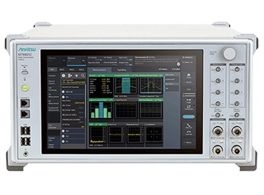
Bengaluru, 26th July, 2017: TUV Rheinland India, a subsidiary of TUV Rheinland Group, Germany, a worldwide leader in Testing, Training, Inspection, Consulting & Certification, announced that it has achieved another milestone by adding the long range testing & certification activities for the Indian market. With the introduction of CMW 500 signalling unit and available infrastructure of its 10m anechoic chamber, TUV Rheinland India can now offer, complete testing & certification services for 2G, 3G, and 4G cellular etc. for various applications.

“We are extremely pleased that this is one of the unique services offered amongst our competitors and the first to be offered in TR – Group companies”, said Thomas Fuhrmann, Managing Director, TUV Rheinland India. “With this facility & necessary accreditations like A2LA, ISO 17025, FCC & IC in place, we can actively cover complete short range & long range testing & certification activities from India, which covers the complete gambit of regulatory testing services.”

India being one of the fastest growing markets in wireless industry globally, it is estimated that 20 billion connected wireless devices are in use for various sectors of Internet of Things(IoT), be it smart city, smart grid, home automation, automotive wireless, mobile communication, M2M (machine to machine communication), cyber security and so on. Also with India looking forward to make its manufacturing & industries sectors smarter, Industry 4.0 roadmap shall play a major role in automating and secure data exchange in manufacturing technologies.

“With growing demand of wireless technology & increase in the manufacture base for mobile phones, tablet PC, PDAs and various life style products, testing & certification of these devices has become a necessity” said Kalyan Varma, Vice President Products, TUV Rheinland India.“TUV Rheinland India is now completely geared up to offer the testing & certification for complete wireless technologies, while championing the short range wireless testing & certification activities for Wi-Fi, Bluetooth, ZigBee, RFID etc. for various applications designed for world-wide & regional based Industrial, Scientific and Medical (ISM)/Unlicensed bands with all modulations techniques supported as well.”

With survey reports that suggests, India is going to need a minimum of 8 – 10 billion communication modules to be integrated into smart sensors and controllers, and another 10 – 50 million gateways that need to operate and maintain the Nation Wide Critical Infrastructure, with already a staggering 40 million plus telecommunication & long range customer equipment being deployed. The time was right for TUV Rheinland India to scale up their services to cater to the biggest regulatory market.

The services in 2012-13 were initially semi-furnished with non-availability of a long range network simulator to provide the complete in-house test services. In 2014-15, TUV Rheinland India worked together with Standard-Body (3GPP, ETSI, FCC, ILAC, IEEE, etc.) & it members to understand the needs and list of critical components to put-up a very well defined and holistic test suite to emerge as the premium long-range wireless test provider.

“The exploding market for telecommunication products since 1934 has created technological advances that no one could have imagined. By upgrading our testing labs in India, TUV Rheinland has met and continues to meet the demand by industry leaders worldwide for electromagnetic compatibility (EMC) tests as per global industry requirements.” added Kalyan Varma.


The post Wireless Testing & Certification For Long Range Devices appeared first on Electronics For You.


Schottky Barrier Rectifiers Combine Ultra-Low Forward Voltage Drop, High Current Handling and Compact Footprint

$
0
0

Ideal for high-frequency SMPSs and DC-DC converters in demanding automotive applications

Beijing, China, July 26, 2017 —Littelfuse, Inc., the global leader in circuit protection, today introduced a series of Schottky Barrier Rectifiers designed to outperform conventional switching diodes in commercial, industrial and automotive applications. DST Series Schottky Barrier Rectifiers combine ultra-low forward voltage drop, high current handling, high junction temperature capability, and low leakage performance in a compact TO-277B surface mount package. For automotive applications up to 10A, it offers the same or better performance as Schottky Barrier Rectifiers provided in D-PAK packaging, with a footprint that’s only one-third of the size. View the video.

DST Series Schottky Barrier Rectifiers

Typical applications for DST Series Schottky Barrier Rectifiers include high-frequency switch-mode power supplies (SMPSs) and DC-DC converters found in automotive applications such as Advanced Driver Assistance Systems (ADAS) (such as cameras, sensors, and electronic control units), infotainment systems (GPS, audio, etc.), LCD displays, and LED headlights and tail lights. Other applications include polarity protection diodes and reverse blocking diodes.

“The DST Series of Schottky Barrier Rectifiers includes devices that are AEC-Q qualified and manufactured in accordance with the TS/ISO16949 automotive quality management system standard,” said Zhiwei Wang, product manager at Littelfuse. “That means circuit designers for the automotive industry can design these parts into their next generation of products with confidence.”

DST Series Schottky Barrier Rectifiers offer these key benefits:
• Ultra-low forward voltage drop (VF) reduces thermal and electrical conduction losses, thereby improving system efficiency.
• Provide high-speed switching for use in very high-frequency applications with minimal switching loss.
• High junction temperature capability ensures high reliability in high ambient temperatures and applications with minimal cooling available.


The post Schottky Barrier Rectifiers Combine Ultra-Low Forward Voltage Drop, High Current Handling and Compact Footprint appeared first on Electronics For You.

DIY: NE555 timer circuit

Self-Healing Electronics: On The Way

$
0
0

As electronic devices are evolving to perform more sophisticated tasks, manufacturers are packing as much density onto a chip as possible. However, such density causes reliability problems such as failure stemming from fluctuating temperature cycles as the device operates or fatigues. A failure at any point in the circuit can shut down the whole device.

However, there is only so much you can do to manually repair a modern sophisticated electronic device, as sometimes you cannot even get to the insides of such a device. For example, in a multilayered integrated circuit, there is no way to open it up. Normally, you would just replace the whole chip.

This is true for a battery, too. You cannot pull a battery apart to try to find the source of the failure. Most consumer devices are meant to be replaced with some frequency, adding to electronic waste issues, but in many important applications such as instruments or vehicles for space or military functions, electrical failures cannot be replaced or repaired.

Breaking of materials with minor or major faults in electronic devices leads to their malfunctioning. These material faults can be rectified by an expert technician on the job, but this would lead to a vicious circle of exploitation and might eventually force you to discard the faulty electronic device prematurely. When one tiny circuit within an integrated chip cracks or fails, the whole chip or the whole device is a loss. But what if it could fix itself, and fix itself so fast that you never even know there was a problem?

Electronic materials have been a major stumbling block in the advancement of flexible electronics because existing materials do not function well after breaking and re-making. Electronic devices are subjected to mechanical deformation over time, which could destroy or break these.

Self-healing materials are a class of smart materials that have the structurally-incorporated ability to repair the damage caused by mechanical usage over time. The inspiration comes from biological systems, which have the ability to heal after being wounded. A team of engineers has developed a self-healing system that restores electrical conductivity to a cracked circuit in less time than it takes to blink. Rather than having to build in redundancies or a sensory diagnostics system, this material is designed to take care of the problem itself.

Researchers have developed a flexible electronic material that self-heals to restore many functions, even after multiple breaks. Here, the material is shown being cut in half. The healed material is still able to stretch and hold weight (Image courtesy: Qing Wang/Penn State)

Electronics requirements from self-healing materials

Self-healable materials are those that, after withstanding physical deformation such as being cut in half, naturally repair themselves with little to no external influence. The new electronic material created, however, can heal all its functions automatically even after breaking multiple times. This material could improve the durability of not only wearable electronics but all other electronic devices.

In the past, researchers have been able to create self-healable materials that can restore one function after breaking, but restoring a suite of functions is critical for creating effective wearable electronics. For example, if a dielectric material retains its electrical resistivity after self-healing and not its thermal conductivity, it could put electronics at the risk of over-heating. This is the first time that a self-healable material has been created that can restore multiple properties over multiple breaks—this could be useful across many applications.

Technology fundamentals

Electronic conductivity. Of late, there has been a big research push aimed at developing self-repairing, electrically-conductive materials that can withstand the damage caused by the twisting and deformation of materials. But so far, most of that research has focused on self-repairing electrical conductors. The team previously developed a system for self-healing polymer materials and decided to adapt their technique for conductive systems. It dispersed tiny microcapsules, as small as ten microns in diameter, on top of a gold line functioning as a circuit. As a crack propagated, microcapsules broke open and released the liquid metal contained inside. The liquid metal filled the gap in the circuit, restoring electrical flow.

This is one example of taking the microcapsule based healing approach and applying it to a new function. Everything prior to this has been on structural repair. This is on conductivity restoration. It shows that the concept translates to other things as well. A failure interrupts the current for mere microseconds as liquid metal immediately fills the crack.

The researchers demonstrated that 90 per cent of their samples healed to 99 per cent of original conductivity, even with a small amount of microcapsules. The self-healing system also has the advantages of being localised and autonomous. Only microcapsules that a crack intercepts are opened, so repair only takes place at the point of damage. Further, it requires no human intervention or diagnostics—a boon for applications where accessing a break for repair is impossible, such as a battery, or finding the source of a failure is difficult, such as an aircraft or a spacecraft.

The post Self-Healing Electronics: On The Way appeared first on Electronics For You.

Low Power, High Efficiency PMICs Extend Battery Life For Hearables MAX77650/MAX77651

$
0
0

MAX77650 and MAX77651 with single inductor multi-output regulator and
charger are optimized for small Li-ion batteries

San Jose, CA—July 26, 2017—Designers of Bluetooth® headphones, activity monitors, smart garments, smartwatches, and other size-constrained devices can now increase battery life and efficiency using the MAX77650 / MAX77651 power management ICs (PMICs) from Maxim Integrated Products, Inc.

Size is critical for hearables and wearables as they continue moving to smaller form factors. Most PMICs for these small, lithium-ion battery-operated devices require additional components, such as boost, buck, and low dropout (LDO) regulators; a charger; and current regulators for LED indicators. For space-savings and efficiency, Maxim has integrated all these functions into a complete power solution that is only 19.2mm-squared—less than 1/2 the size of existing component combinations.

The MAX77650 and MAX77651 feature single inductor multiple output (SIMO) buck-boost regulators that provide three independently programmable power rails from a single inductor, 150mA LDO, and three current sink drivers to reduce overall component count and maximize available board space. For design flexibility, the MAX77650 operates up to 3.3V and the MAX77651 operates up to 5V—both include an analog multiplexer (MUX) output for safe battery monitoring, making them ideal for low-power designs.

Key Advantages

Lowest Standby Power: 0.3µA; 5.6µA operating current

High Efficiency: 3-output SIMO channels plus LDO extend Li+ battery life

Smallest Solution Size: Multi-channel SIMO regulator reduces component count

Commentary

  • “The MAX77650 offers a lot of functionality for highly integrated wearable products, which allows us to make the next leap in reducing the size of Bluetooth music headsets,” said Tjapko Uildriks, CEO, Dopple B.V. “The MAX77650 integrates many essential power management features typically found in advanced wearable products, enabling Dopple to build high-quality Bluetooth music headset platforms.”
  •  “Demand for consumer battery management ICs is expected to grow at a CAGR of 5% from 2017 to 2020,” said Richard Eden, Senior Analyst, Power Semiconductors, IHS Markit Technology. “Among consumer applications, battery management for wearables—which includes hearables—shows the fastest CAGR of 29% over the same 3-year period.”
  • “Maxim has leveraged its PMIC expertise to offer its smallest ultra-low power, battery-charging solutions with the MAX77650 and MAX77651, which are well positioned to take advantage of the projected market growth,” said Scott Kim, Executive Business Manager, Mobile Power, Maxim Integrated. “While we optimized the MAX77650 and MAX77651 for small battery size, we also include numerous factory programmable options that allow our customers to tailor these solutions to their requirements and get to market faster.”


The post Low Power, High Efficiency PMICs Extend Battery Life For Hearables MAX77650/MAX77651 appeared first on Electronics For You.

Electronic System Design: Begin With XSCHEM

$
0
0

The need for a schematic editor arises from the complex electronic systems that were once manually drawn by engineers and designers. Today, most modern schematic software are equipped with state-of-the-art tools that can handle very complex circuit conception to its final product. This is how digital schematics were born.

XSCHEM could be that tool of choice that lets you work with nets, pins and wires. Knowing these basics marks the beginning of formal circuit design followed by simulation. During the first step in a design cycle, you have to make sure that the tools in the schematic editor are well understood. Once the schematic has been drawn on the computer, circuit connectivity and device netlist are generated and sent to a circuit simulator.

Judging a book by its cover

To make this process effective while transcending the concept from your mind to the editor, an easy graphical interface is required. By focusing on interfaces, hierarchy and instance properties, this software helps simplify a complex system and creates an illustration that looks like small building blocks of the project.

XSCHEM is made more attractive by its capability to handle integrated circuit (IC) design and to generate netlists for very-large-scale digital, analogue or mixed-mode simulations.

A netlist is generated with every simulation, and that provides a textual description of a circuit made of components. Components such as gates, resistors, capacitors and transistors can all be listed together to form a netlist when used in analogue simulation tools. Once the schematic is created, a circuit netlist can be generated for simulation.

Currently, XSCHEM supports three netlist formats:
• SPICE netlist
• VHDL netlist
• VERILOG netlist

Give the benefit of the doubt

XSCHEM could be looked upon as a featureful industrial-grade software. As you can see in Fig. 1, it is a depiction of VLSI system(s)-on-chip imported in XSCHEM. In the figure, the tool is seen handling more than ten hierarchies, and the primary goal of this program is to build a bigger schematic. This has been the primary goal during the whole development of the program.

Analogue circuit example
Fig. 1: Analogue circuit example

Although the user interface looks very simple, the net-listing and rendering engines in XSCHEM are designed from the ground up to handle very large designs in the most efficient way. All you have to do is keep bind keys in your hands, as most of the work is done by these. This comes in very handy when working on bigger projects that combine more than 1000 transistors and still use context menus and elaborate graphical actions while designing these.

Start designing using layers

Most editing commands are available in the menu, but definitely key bindings and mouse actions are the most effective ways to build and arrange schematics, so you should learn at least the most important ones.

Properties are text strings that are associated with XSCHEM objects. All graphic primitives such as lines and wires, which could be combined to create more complex graphical images, are supported. These are:
• Wires
• Lines
• Rectangles
• Texts

Consider, for example, res.sym symbol (you may open it with Open menu). If you click on one of the red pins and press edit property bind key q, a dialogue box shows the property string associated with the selected pin.

Wire layer.

Wiring is one of the most important aspects of an electrical design. In this software the wires are said to be equivalent of copper traces found in printed circuit boards or electrical conductors. The wires can be drawn as lines while the electrical connectivity graph is built by the software itself. If you wish to draw a wire segment, all you have to do is point the mouse somewhere on the drawing window and press w key.

It could be seen that an elastic wire image appears with one end following the mouse cursor. By clicking the left mouse button, the wire could be brought to the place where it needs to be finished. XSCHEM has an advanced way of recognising the connection of wires, and uses this information to build circuit connectivity. Hence, all wires are drawn from the wire layer.

Text layer.

It is easy to place text on the design pane. All you have to do is use shortcut bind key t to enable text feature. This opens up a dialogue box, which appears where you can provide inputs as text and determine text size.

Line layer.

While using XSCHEM you will get familiar with layers as every component in the design is part of a layer. Every layer has its own characteristic like colour and hierarchy. Lines in this software do not have any electrical meaning and are just segments for drawing lines. XCHEM has provisions that make lines look like wires, which could be implemented using bind key l.

Rectangles layer.

Fig. 2: Digital system for VHDL simulation | XSCHEM
Fig. 2: Digital system for VHDL simulation

While drawing rectangles, again on multiple layers, a specific PIN layer is used to make pins that are used to interconnect wires and components. Rectangles are placed with bind key r on the design screen.

The post Electronic System Design: Begin With XSCHEM appeared first on Electronics For You.

Serial Interface Using Python Software

$
0
0

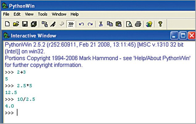
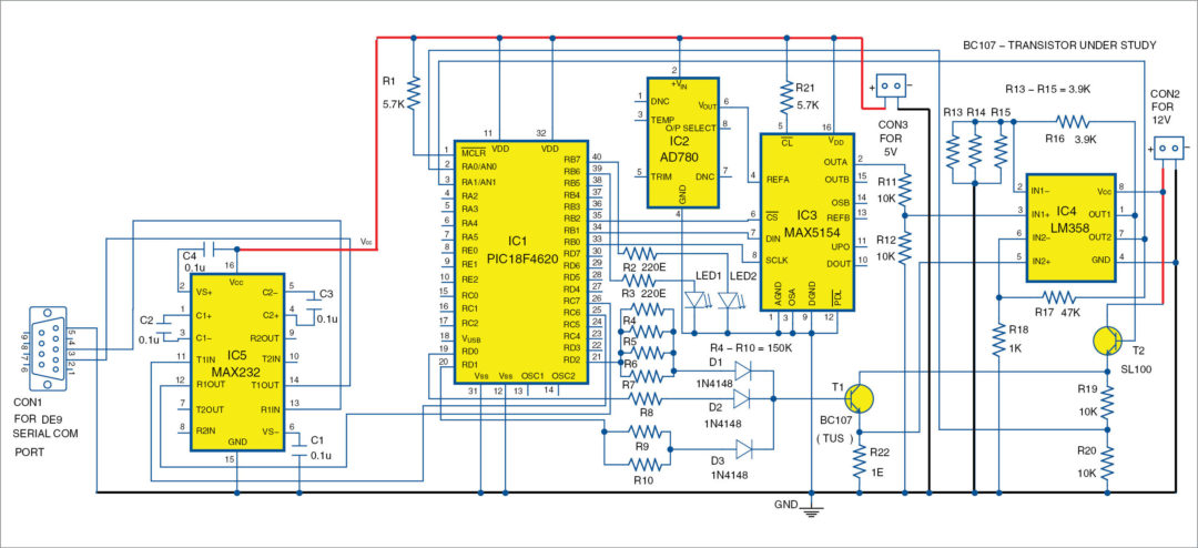
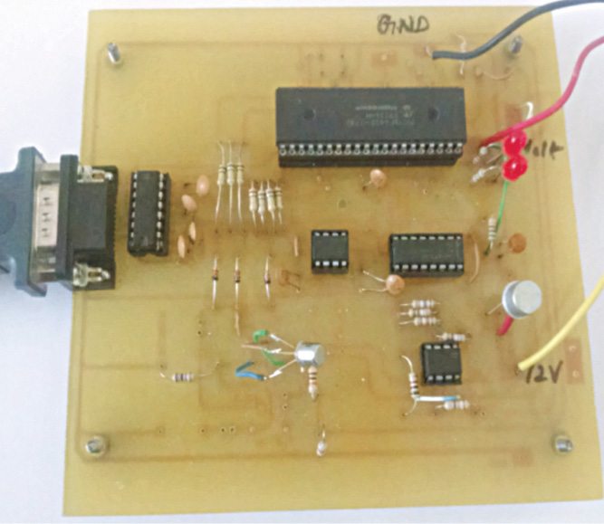
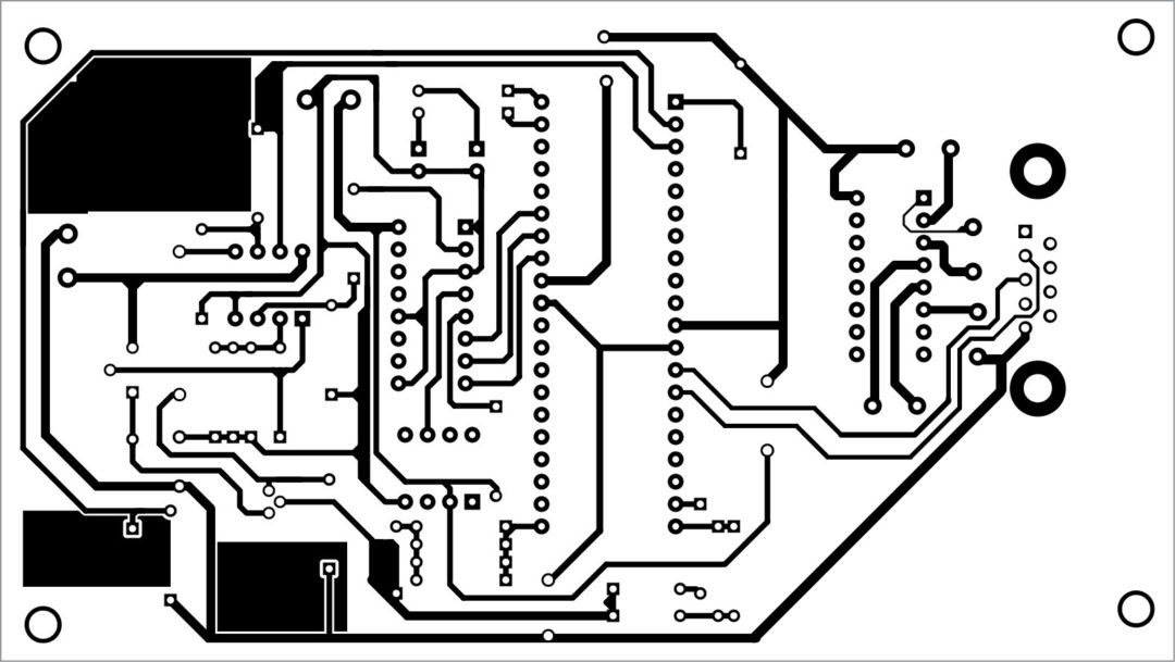
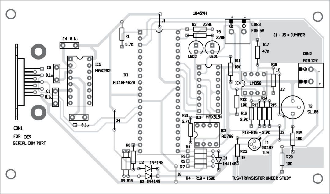
Presented here is a project for a simple transistor’s output characteristic curve-tracer program through the serial interface and PIC microcontroller using Python programming language. Output characteristic curve of a transistor is automated using Python software and serial interface. Application software for collecting the measured value and displaying it on the monitor screen is developed using Python.

Engineers and academicians have been using high-level languages like Visual C++, Visual Basic and Delphi for connecting their gadgets/embedded systems with the computer for measurement and control purposes for a long time. Recently, many shifted their preference to Python as their computer language for measurement and analysis. The main advantage of using Python is the support of a large open source community.

Python is an interpreted programming language like BASIC, which saves considerable time during program development because compilation and linking are not required. Programs written in Python are typically much shorter as compared to ones written in C or C++.

Python can be used for writing standalone programs and scripting applications. It is free, portable, powerful and remarkably easy to use.

To run a Python program, an interpreter is required. Python interpreter is a program that reads a Python program and then executes it. To write a Python program, it is advisable to use an editor (for typing a program). An editor is designed for writing Python programs. It provides highlighting and indentation that can help you write a program without mistake.
The interpreter can be used to experiment with different features of the language. There are two modes in which interpreters can be used, namely, interactive and script. In interactive mode, the interpreter prints the result as the program is typed. The chevron, >>>, is the prompt the interpreter uses to indicate that it is ready.

Alternatively, you can store the code in a file and use the interpreter to execute the contents of the file, which is called a script. By convention, Python scripts end with .py extension. (Python installation package is available at http://python.org)

Writing the first Python program

After the installation of Python IDE and PyWin32 software, you can write a program and run it. The traditional first program is Hello World. This program simply prints ‘Hello World’ on the screen when it is run. This can be done with one statement in Python, as shown in Fig. 1.

Printing ‘Hello World’ on PythonWin window
Fig. 1: Printing ‘Hello World’ on PythonWin window

Mathematical operations are performed in a single line without declaring the variables involved, as shown in Fig. 2.

Interactive Python Shell
Fig. 2: Interactive Python Shell

Circuit and working

Circuit diagram of the serial interface and transistor curve tracer is shown in Fig. 3. The author’s prototype is shown in Fig. 4. The circuit consists of a PIC18F4620 microcontroller (IC1), AD780 voltage regulator (IC2), MAX5154 12-bit digital-to-analogue converter, also called DAC (IC3), LM358 voltage amplifier (IC4), MAX232 dual driver/receiver (IC5), power transistor SL100/CL100 (T2), BC107 transistor-under-study (TUS) and other essential components needed for microcontroller operations.

Circuit diagram of the serial interface and transistor curve tracer
Fig. 3: Circuit diagram of the serial interface and transistor curve tracer

Clock frequency required for microcontroller operation is derived from its internal oscillator. Base current of TUS (T1) is varied from 0µA to 175µA in eight steps using port D pins (RD0, RD1 and RD2) of IC1. Collector voltage of T1 is varied from 0V to 2.5V in eight steps using IC1 and IC3 through IC4 and T2. Output voltage from the DAC is amplified about four times using LM358 and given to the base of T2.

Author’s serial interface using Python software prototype
Fig. 4: Author’s prototype

Emitter of T2 is connected to the collector of TUS, whose voltage is being varied. Collector voltage of TUS is given to channel-0 (AN0) of the built-in analogue-to-digital converter (ADC) of IC1 after dividing the voltage by half using a potential divider arrangement (R19 and R20) to meet the voltage limitation of the microcontroller.

Assuming that the collector current of TUS is equal to its emitter current, output is taken across the 1-ohm resistance, and the drop across 1-ohm resistance is amplified about 50 times and given to channel-1(AN1) of the built-in ADC of IC1.

Construction

An actual-size, single-side PCB layout for the USB interface is shown in Fig. 5 and its component layout in Fig. 6. After assembling the circuit on the PCB, enclose it in a suitable box.

PCB layout of the serial interface using Python software
Fig. 5: PCB layout of the serial interface using Python software
Fig. 6: Component layout of the PCB

Firmware

The firmware is written in C and compiled using CCS C compiler. It implements the following tasks:
1. Generates different base currents
2. Generates different collector voltages
3. Measures the voltage and current (current in terms of voltage)
4. Sends the data to the PC

Host software

The application software to collect the measured value and display it on the monitor screen has been developed using Python. It requires the following components to be installed on your system: Python 2.5 (python-2.5.2) or higher IDE, Win32 Python (pywin32-210.win32-py2.5), Serial Port (pyserial-2.2.win32), Matplot Library (matplotlib-0.91.2.win32-Py2.5) and Numeric Python (numpy-1.0.4.win32-py2.5). Output pattern is displayed using Tkinter software, and values are displayed in a text file. Tkinter software is a part of Python package, so there is no need to separately install it.

The post Serial Interface Using Python Software appeared first on Electronics For You.

Tutorial: 3 Coil DC Motor


Wireless Gate Alarm

$
0
0

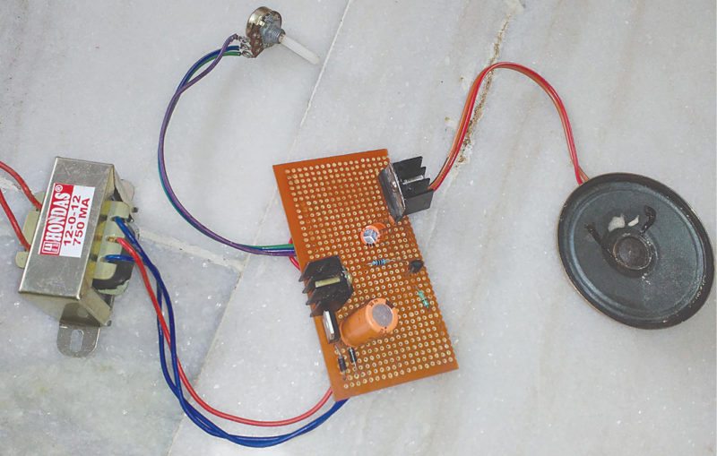
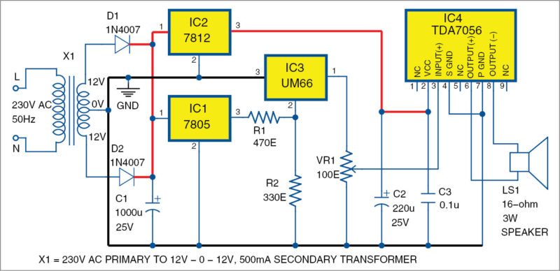
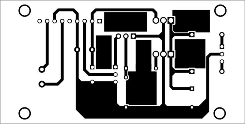
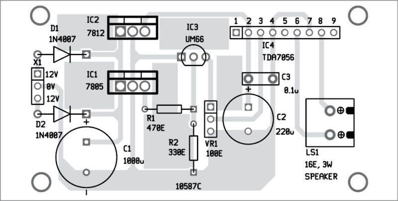
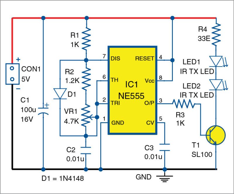
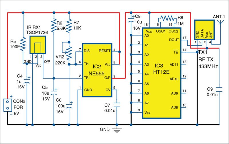
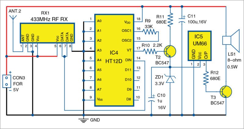
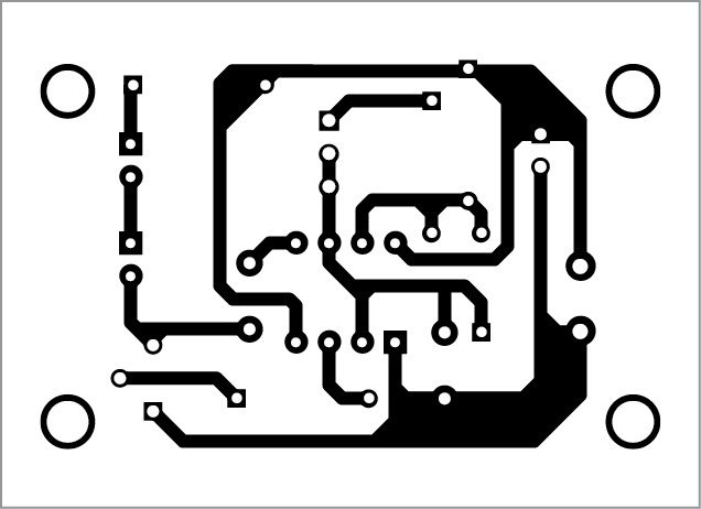
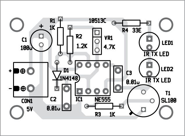
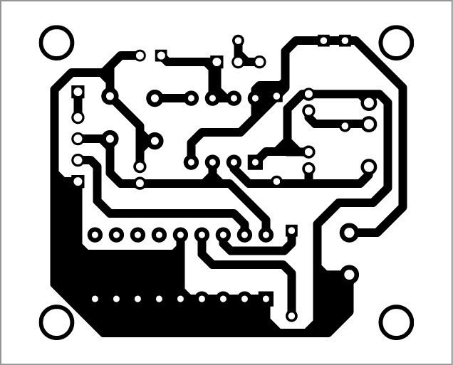
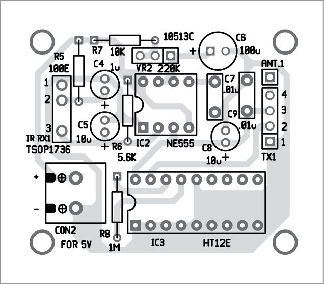
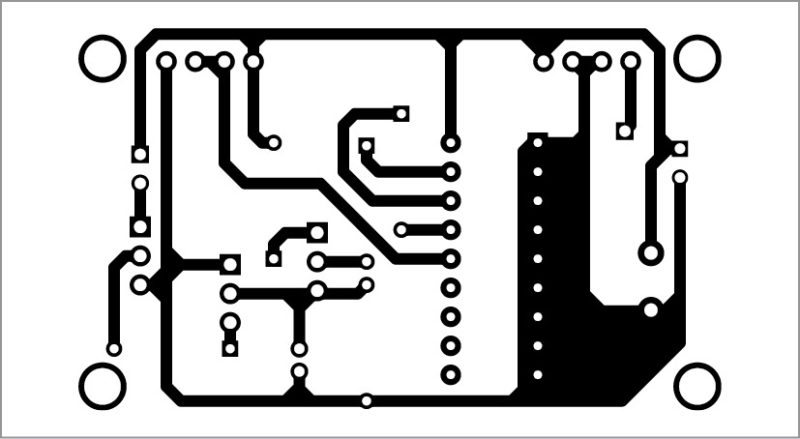
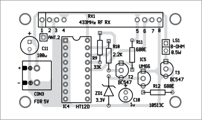
This wireless gate alarm uses infrared (IR) and 433MHz RF modules. IR transmitter unit emits 36kHz signal and is fitted on one side of the gate’s frame. IR receiver unit and RF transmitter module, along with the encoder, are fitted on the opposite side of the gate’s frame. The alarm unit is kept inside the house, and it uses 433MHz RF receiver module and musical alarm circuit.

Circuit and working

Circuit of the wireless gate alarm has three units, namely, IR transmitter unit, IR receiver unit and alarm unit. Modulated invisible IR beam is present between transmitter and receiver units installed at the gate.

Circuit diagram of the IR transmitter unit is shown in Fig. 1. By adjusting potmeter VR1, frequency can be set at 36kHz. At this frequency, maximum range is obtained (more than five metres).

Circuit diagram of the IR transmitter unit
Fig. 1: Circuit diagram of the IR transmitter unit

IC NE555 (IC1) is wired as an astable multivibrator. Output signal from NE555 is amplified by npn transistor SL100 (T1) to drive two IR-transmitting LEDs (LED1 and LED2) in series.
Circuit diagram of the IR receiver unit is shown in Fig. 2. It is built around IR receiver module TSOP1736 (IR RX1), timer NE555 (IC2), encoder HT12E (IC3), 433MHz RF transmitter module (TX1) and some other components.

Circuit diagram of the IR receiver unit
Fig. 2: Circuit diagram of the IR receiver unit

Circuit diagram of the alarm unit is shown in Fig. 3. It is built around 433MHz RF receiver module (RX1), decoder HT12D (IC4), melody generator UM66 (IC5) and some other components.

Circuit diagram of the alarm unit
Fig. 3: Circuit diagram of the alarm unit

Encoder IC3 encodes four-channel transmitting signals. The address pins A0 through A7 of IC3 are used for security codes. Here, all the address pins are grounded. Decoder IC4 decodes four-channel signals. IC3 has the same address pins as IC4.

When a person crosses the gate, IR beam is interrupted for a moment. Then, output of TSOP1736 sensor goes high. IC2 gets triggered and output pin 3 goes high.

This output signal of around 5V is applied to IC3 and TX1, which transmits the signals to the remote alarm unit. The transmitted signal received by RX1 is fed to pin 14 (DIN) of IC4. Pin 17 of IC4 goes high when a valid RF transmission signal is received.

Transistor T2 (BC547) conducts when pin 17 of IC4 goes high. When T2 conducts, IC5 gets power supply and it produces an alarm sound through loudspeaker LS1.

Construction and testing

An actual-size, single-side PCB layout for the IR transmitter unit is shown in Fig. 4 and its component layout in Fig. 5. Assemble the unit in a suitable enclosure and fix on the frame of the gate.

PCB layout of the IR transmitter unit
Fig. 4: PCB layout of the IR transmitter unit
 Component layout of the IR transmitter unit PCB
Fig. 5: Component layout of the PCB shown in Fig. 4

An actual-size, single-side PCB for the IR receiving unit is shown in Fig. 6 and its component layout in Fig. 7. Assemble the unit in a suitable enclosure and fit at the other side of the gate.

PCB layout of the IR receiver unit
Fig. 6: PCB layout of the IR receiver unit
Component layout of the IR receiver unit PCB
Fig. 7: Component layout of the PCB shown in Fig. 6

An actual-size, single-side PCB layout for the alarm unit is shown in Fig. 8 and its component layout in Fig. 9. Assemble the unit in a suitable enclosure and keep it inside the house.

PCB layout of the alarm unit
Fig. 8: PCB layout of the alarm unit
Component layout of the alarm unit PCB
Fig. 9: Component layout of the PCB shown in Fig. 8

All three units work on 5V DC power supply. Use an antenna for transmitter and receiver RF modules; a 17cm single-strand hook-up wire can be used as the antenna.

Download PCB and component layout PDFs: click here


The post Wireless Gate Alarm appeared first on Electronics For You.

Cyber Standards | Smartphones | End to End IoT Security

$
0
0

New Cyber Standards for IoT Ease – But Won’t Solve – Security Challenge

The first independent standard for cybersecurity for the Internet of Things (IoT) was approved earlier this month, following two years of debate and discussion over how to measure and secure such devices.

The American National Standards Institute (ANSI) approved UL 2900-1, General Requirements for Software Cybersecurity for Network-Connectable Products, as a standard on July 5. The effort was spearheaded by Underwriters Laboratories (UL), which is preparing two more standards to follow: UL 2900-2-1, which defines requirements for network-connectable components of healthcare systems, and UL 2900-2-2, which does the same for industrial control systems.

The three establish the first standard security protocols for software-controlled IoT devices, such as access controls, industrial controls for lighting and mechanical systems, internet-connected medical devices and more. They also offer potential answers to major worries about the lack of security built into such devices thus far. (Read More)


Are Smartphones Threatening the Security of our IoT Devices?

By 2020, the number of Internet of Things devices is estimated to surpass 20 billion. From smart fridges to coffee makers and Barbie dolls, connected things will soon fill our households. Many of these devices are, and will continue to be, accessed via our smartphones. While this is very convenient for users, there are weaknesses in smartphone security that can be exploited to turn smart objects against us. While many of us are now well acquainted with best practice when it comes to using laptops or desktops, it is easy to be somewhat lax when it comes to our phones.

Recent years have seen an upsurge in internet-connected medical devices and fitness trackers, many of which feed data to or can be controlled via apps on our phones. This means that such devices now contain valuable data about our health and wellbeing that are vulnerable to cyberattacks. IoT objects increasingly rely on smart devices with sensors built in and applications to support them. (Read More)


Mocana Teams Up with Gemalto to Secure IoT from End to End

Mocana, a provider of critical security solutions for industrial control systems (ICS) and the Internet of Things (IoT) and Gemalto, a leader in IoT and digital security, have together announced a new partnership to bring connectivity, security and monetization to IoT deployments. The two companies will provide an end-to-end solution for IoT security lifecycle management, including interoperability of Mocana’s IoT Security Platform and Gemalto’s digital security products to protect data and digital identities across endpoint devices, gateways and clouds. Combining the companies’ respective areas of expertise makes it easier for manufacturers, enterprises and service providers to build strong security into IoT devices and critical infrastructure that are vulnerable to cyber-attacks.

Gemalto and Mocana will leverage their solutions and global ecosystems with the goal of making it easier to embed advanced cybersecurity technologies into IoT devices, industrial control systems, and machine-to-machine (M2M) networks. (Read More)


The post Cyber Standards | Smartphones | End to End IoT Security appeared first on Electronics For You.

IOT Based Power Outlet | Home Automation

$
0
0

This video is around WeMOS and demonstrates how to use WeMOS with thingspeak to control loads in the home. This project lets you control your devices which you need to connect to the output sockets. As an online server, the presenter has used Thinspeak but you can use any server (you just need REST API). Check out the video to get started.

GitHub Repository: click here

Schematic


The post IOT Based Power Outlet | Home Automation appeared first on Electronics For You.

Integration is a big issue in IoT device deployment

$
0
0

Telit is an enabler of machine-to-machine (M2M) communications worldwide providing wireless module technology, services and connectivity. It offers integrated products, platforms and services to support and enable IoT deployments from things to apps. Ashish Gulati, country manager for Telit, speaks to EFY’s Dilin Anand about how cellular technologies are evolving with the Internet of Things (IoT) and growth of connected devices


Ashish Gulati, country manager at Telit Wireless Solutions

Q. What trends do you observe in Wireless Technologies for M2M?

A. For IoT modules, we have different cellular technologies. Today, Long Term Evolution (LTE) technology accounts for half of our customers. The other half of the demand is mostly for 3G, with 2G accounting for almost none. This was not the case in 2012.

Q. Is India network-ready for IoT deployment?

A. Usually, it takes 18-24 months for a cellular operator to launch a commercialised cellular network. In June last year, 3GPP body finalised the narrow-band IoT (NB-IOT) and Cat-M1 specifications. Operators in North America try to commercialise network services in 6-12 months (instead of 24 months). Given that, they are hard pressed on timelines to offer this network as Cat-M1 is still under field trials in North America.

In India, most LTE operators have their networks compliant to Cat-1. And they have started working towards NB-IOT and Cat-M1 even before Cat-1 becomes widespread.

Q. What’s the cost impact of wireless evolution?

A. If the module is going to change, you have to change the antennae as these are different for 2G, 3G and LTE. Then there are some minor changes in the power supply. The rest of the changes are on the software side. So overall bill-of-materials (BOM) cost is more or less the same.

Q. How easy is it for product teams to switch their designs from one module to another?

A. Customers must share the application or product that they are using right now. Our modules are AT command driven. When a customer tells us what product they are using, we compare AT commands that are different. While most are common, some proprietary commands may differ. We review these and tell our customers the changes that they need to make to straightaway use our modules. Thus, it becomes very easy for customers.

Q. What are the issues faced in deployment of IoT solutions?

A. I see more of integration issues because in certain cases it is difficult to integrate IoT devices with the conventional equipment/machinery in a manufacturing plant. For instance, sometimes there are older equipment that have no relevant data outlet, so we must create one in such cases.

Q. What help do you provide to independent design houses?

A. We go much beyond supporting independent design houses (IDHs) on their design initiatives. In some cases we help them showcase their product solutions to global market through industry exhibitions. We sign up agreements with IDHs, whereby we work with them exclusively for an application and promote it to prospective clients. We also introduce them to our distribution partners for joint promotional campaigns.

For reading the full interview: Click here


The post Integration is a big issue in IoT device deployment appeared first on Electronics For You.

What do you know about Synaptic Transistors?

$
0
0

It is a well-known fact that the highly remarkable supercomputers are power-hungry and staggeringly inefficient machines. In the meantime, our brains consist of about 86 billion neurons that are connected by synapses that not only establish myriad logic circuits, but also adapt to stimuli continuously strengthening few connections while weakening others. We call this process learning and it enables highly efficient and rapid computational processes. Material scientists At SEAS (Harvard School of Engineering and Applied Sciences) have now developed a new kind of transistor that mimics the synapse’s behavior. A synapse is defined as a junction between 2 nerve cells that consists of a minute gap. The impulses pass across this gap by the diffusion of a neurotransmitter. In a circuit, the synaptic transistor modulates the flow of information along with physically adapting to changing signals.

Several Prototypes of Synaptic Transistor can be seen on this Silicon Chip. Image: Eliza Grinnell, SEAS Communications
Several Prototypes of Synaptic Transistor can be seen on this Silicon Chip. (Image Courtesy: Eliza Grinnell, SEAS) Communications

The synaptic transistor can mark the emergence of a new type of artificial intelligence(one embedded in the very architecture of a computer but not in smart algorithms) by exploiting the modern materials’ unusual properties.

Shriram Ramanathan, associate professor, materials science, Harvard SEAS, says, “Nowadays, there is an extraordinary interest in developing energy-efficient electronics. Historically, the major focus of people had been on speed but with speed comes the dissipation of power. With electronics becoming highly ubiquitous and powerful, you could have a large impact by decreasing the amount of energy they consume.”

For all of its magnificent computing power, the human mind runs on around twenty watts of energy (lesser than a household light bulb), so it provides a natural model for engineers.

In a human brain, transistor is analogous to a synapse. Each time a neuron instigates an action and the other neuron retaliates, the strength of their connection is increased by the synapse between them. The strength of a synaptic connection depends on how fast the neurons spike each time. The Synapse memorizes the action between the neurons.

A system that integrates millions of neuron terminals and tiny synaptic transistors can take the parallel computing into a whole new era of high and ultra-efficient performance.

In a biological synapse, while receptors and calcium ions effect a change, the artificial version attains the same plasticity with oxygen ions. These ions slip in and out of crystal lattice of samarium nickelate thin film when a voltage is applied. This thin film acts as the synapse channel between two “dendrite” and “axon” terminals. In the nickelate, the varying concentration of ions lowers or rises its conductance. This implies, the capability of nickelate to carry information on an electrical current. The strength of the connection is based on time delay in the electrical signal just as in a natural synapse.

The synaptic transistor consists of a nickelate semiconductor adjacent to a tiny pocket of ionic liquid and sandwiched between 2 platinum electrodes. The time delay is converted into a magnitude of voltage by an external circuit multiplexer. This voltage is applied to the ionic liquid generating an electric field that either removes the ions or drives them into the nickelate. The whole device with a length of few hundred microns is embedded in a silicon chip.

When compared with the traditional silicon transistors, the synaptic transistor provides several immediate advantages. It is not restricted to the binary system of zeros and ones.

As the material composition changes, this system alters its conductance gradually. Using traditional circuit technology like CMOS would be rather challenging to imitate a synapse as the real biological synapses consist of an unlimited number of possible states – not just ‘on’ and ‘off.’

Non-volatile memory is another advantage that is offered by a synaptic transistor. Non-volatile memory indicates that the device remembers its state even when the power is interrupted.

Besides, the new transistor is essentially energy efficient. The correlated electron systems is an unusual class of materials to which the nickelate belongs. The correlated electron systems can undergo a metal-insulator transition. The material’s conductance changes suddenly when exposed to an external field – at a certain temperature.

This material’s extreme sensitivity is highly exploited. A very small excitation enables you to acquire a large signal, so the input energy needed to drive this switching is very small. For energy efficiency, this could translate into a large boost. For seamless integration into the present silicon-based systems, the nickelate system is positioned correctly.

The big advantage with this kind of device is that the ‘learning’ behavior is more or less temperature insensitive. We can operate this device anywhere within the temperatures starting from the room temperature to almost 160 degrees celsius.

The post What do you know about Synaptic Transistors? appeared first on Electronics For You.

Augmented Reality: How Real is the Interaction

$
0
0

Not many people were aware of the concept of augmented reality until Pokémon Go came in to the picture. This game has been taking the world by storm. Augmented reality uses techniques to expand the real world outside your imagination. Many Android and iOS apps are now being designed using the principle of augmented reality.

Augmented Reality is an absolute or composite view of the physical or real environment superimposed with virtual elements that have been enhanced by computer-generated sensory input like sound, video, graphics and GPS. You can digitally manipulate the information about your surroundings in real time using the phenomenal augmented reality technology.

Concept of augmented reality
Fig. 1: Concept of augmented reality

Key characteristics of augmented reality are:
1. Overlapping of real and digital worlds
2. Registration and alignment in 3D
3. Real-time interaction

Characteristics of augmented reality
Fig. 2: Characteristics of augmented reality

Augmented reality is already being used in many areas, some of which are:

Virtual dressing rooms.

This is an augmented reality based dressing room application, where you can select your favourite clothes and accessories virtually without buying or even trying these on physically.

In military camps.

In combat, augmented reality can serve as a networked technology for the communication system that assimilates useful battlefield data onto a soldier’s goggles in real time. From the soldier’s view, people and various objects can be marked with special indicators to warn of potential dangers. The map evokes the layers of the indicated trajectories for various objects in geographic coordinates. It supports telescope operators in identifying satellites and cataloguing potentially-dangerous Space debris.

The system combines geographic data including street names, points of interest, railroads and airports with live video from the camera system. The system offers images in picture mode that allow it to evoke a general view of the arena that is surrounding the camera’s field-of-view.

Alive app by Times of India.

Alive is an augmented reality based application used to view extensive content like animation, video and photo shoots. You can scan a printed image in newspapers, brochures, pamphlets or magazines, and the app recognises images, logos, location, QR codes and objects in real time.

Components of augmented reality
Fig. 3: Components of augmented reality

How augmented reality works

This technology works on the basis of two types of approaches: marker based and location based.

Marker based augmented reality.

The QR code system is one of the most common methods of marker based augmented reality. It consists of black squares arranged in a square grid on a white background, which can be easily read by an imaging device such as a camera. For this to work, you need a smartphone that has a marker based augmented reality application like QR Code that can scan a pattern such as a barcode or symbol through the camera of the mobile.

The software recognises the pattern and superimposes a digital image on your mobile screen, and gives you a 3D or an animated digital image for a better experience as compared to a 2D image.

Marker based augmented reality application
Fig. 4: Marker based augmented reality application

Location based augmented reality.

With a smartphone and a location based application system like GPS, you can point the augmented reality based application towards a real scene. GPS software recognises the device location in the application. Based on the recorded location and orientation by the inbuilt sensor of your phone, you can predict the overview data of the relevant location. Digital informative data is matched to the real scene, which is then visible through the device camera.

One such application of the location based augmented reality is navigation. It enhances the effectiveness of augmented navigation devices. Information is displayed on the automobile’s windshield and the system indicates the direction and distance of the destination along with weather and terrain conditions, traffic information and potential hazards.

Location based augmented reality application
Fig. 5: Location based augmented reality application

Superimposition based augmented reality.

In this case, the augmented view is superimposed on the real view of an object. Augmented view is either the scanned image of the real object or the internal view of the object. Applications of this kind of augmented reality are in education, defence, medical and architecture, among others.

Augmented reality as superimposition
Fig. 6: Augmented reality as superimposition

Projection based augmented reality.

With the help of this process, you can project virtual images onto physical objects. This method of having a projection of the virtual image is known as the projection augmented model, or PA model. You can even touch, feel and grasp the virtual image with your hands.

Augmented reality as projection
Fig. 7: Augmented reality as projection

Future scope of augmented reality

Some areas where this technology is being developed are films, the retail sector (the technology is closing the gap between online and offline) and computer games.

The mobile industry is also making use of augmented reality. From smartphones with GPS to wearable technologies, ranging from Google Glass to Apple Watch, this comprehensive application of augmented reality can be expressed with specific apps and micro-location technologies. Already there are many applications that offer the same basic versions of augmented reality techniques.

The post Augmented Reality: How Real is the Interaction appeared first on Electronics For You.

Two New SAM Microcontroller Families with Extensive Connectivity Interface Options

$
0
0

SAM D5x and E5x MCUs provide powerful performance and enhanced security features

2 August 2017, New Delhi, [NASDAQ: MCHP] — The SAM D5x and SAM E5x microcontroller (MCU) families are now available from Microchip Technology Inc. These new 32-b

it MCU families offer extensive connectivity interfaces, powerful performance and robust hardware-based security for a wide variety of applications.

The SAM D5/E5 microcontrollers combine the performance of an ARM Cortex-M4 processor with a Floating Point Unit (FPU). This combination offloads the Central Processing Unit (CPU), increasing system efficiency and enabling process-intensive applications on a low-power platform. Running at up to 120 MHz, the D5x and E5x MCUs feature up to 1 MB of dual-panel Flash with Error Correction Code (ECC), easily enabling live updates with no interruption to the running system. Additionally, these families are available with up to 256 KB of SRAM with ECC, vital to mission-critical applications such as medical devices or server systems.

These new MCUs have multiple interfaces providing design flexibility for even the most demanding connectivity needs. Both families include a Quad Serial Peripheral Interface (QSPI) with an Execute in Place (XIP) feature. This allows the system to use high-performance serial Flash memories, which are both small and inexpensive compared to traditional pin parallel Flash, for external memory needs. The SAM D5/E5 devices also feature a Secure Digital Host Controller (SDHC) for data logging, a Peripheral Touch Controller (PTC) for capacitive touch capabilities and best-in-class active power performance (65 uA/MHz) for applications requiring power efficiency. Additionally, the SAM E5 family includes two CAN-FD ports and a 10/100Mbps Ethernet Media Access Controller (MAC) with IEEE 1588 support, making it well suited for industrial automation, connected home and other Internet of Things (IoT) applications.

Both the SAM D5x and E5x families contain comprehensive cryptographic hardware and software support, enabling developers to incorporate security measures at a design’s inception. Hardware-based security features include a Public Key Cryptographic Controller (PUKCC) supporting Elliptic Curve Cryptography (ECC) and RSA schemes as well as an Advanced Encryption Standard (AES) cipher and Secure Hash Algorithms (SHA).

“Applications are becoming increasingly complex and there is a great need to move to faster MCUs with better connectivity options and flexible peripheral support,” said Rod Drake, vice president of Microchip’s MCU32 business unit. “The SAM D5/E5 microcontrollers provide an excellent migration path for developers wanting a cost-effective solution with powerful performance, comprehensive interface options and built-in security.”

Development support

The SAM E54 Xplained Pro Evaluation Kit is available to kick-start development. The kit incorporates an on-board debugger, as well as additional peripherals, to further ease the design process. All SAM D5x/E5x MCUs are supported by the Atmel Studio 7 Integrated Development Environment (IDE) as well as Atmel START, a free online tool to configure peripherals and software that accelerates development.


The post Two New SAM Microcontroller Families with Extensive Connectivity Interface Options appeared first on Electronics For You.


Industry’s First Platform for 6CA Max Throughput Test

$
0
0

2nd Aug, 2017: Anritsu and Samsung Electronics have been collaborating on LTE / LTE-A heretofore. We jointly conducted a connection verification using Samsung’s LTE modem and MT8821C Radio Communication Analyzer.

Samsung Electronics Co., Ltd has confirmed achieving DL 6CA (256QAM) max T-put (1.2Gbps) for its next-generation LTE modem successfully with Anritsu’s MT8821C Radio Communication Analyzer as industry’s first test platform.

Carrier aggregation is a technology that secures a wide bandwidth and improves the communication rate, and service has already started in countries all over the world. Due to the number of users of smartphones / tablet terminals and the rise of rich content services, the spread of LTE-Advanced is continuously expanding. As non-standalone type 5G service to be operated in cooperation with the cellular system is scheduled to be launched in 2019, introduction of 1 Gbps service which further accelerates the current LTE-Advanced is being planned, and Samsung is proactively proceeding the LTE-Advanced function DL 6CC CA during the process of their development.

MT8821C Radio Communication Analyzer is designed for R&D of mobile devices / user equipment (UE), such as smartphones, tablets and M2M modules. It builds on the technologies of its popular predecessor MT8820C, widely adopted by UE and chipset vendors worldwide and supports multiple wireless technologies ranging from LTE-Advanced features like DL CA up to 6CC, to 3G/2G systems as well as LTE-U/LAA, with its easy-to-use measurement functions for efficient RF parametric and physical layer throughput testing.

“Anritsu is delighted that Samsung, a leader in ASIC and solutions, has confirmed MT8821C as a key tool in their development process”, stated Mr. Tsutomu Tokuke, Head of Mobile Solutions Division at Anritsu. “This progress shows how Anritsu’s MT8821C helps LTE device makers ensure their product quality in an intensely competitive market while reducing the product launch cycle time”.


The post Industry’s First Platform for 6CA Max Throughput Test appeared first on Electronics For You.

IoT-enabled Smart Pumping Solutions for Industries

$
0
0

New Delhi: August 1, 2017 – Schneider Electric, today expanded the range of its smart pumping solutions, under its automation portfolio, with the launch of Altivar, Modicon, and Magelis pumping products. The new devices, when combined with MachineStruxure automation solutions, helps build and manage flexible, connected, and efficient pumping systems across industries such as infrastructure, building, water & wastewater, oil & gas and food & beverage.

The country’s industrial sector constitutes a significant chunk of India’s pumps market with applications across power plants, chemical manufacturing and water & waste water treatment. Government efforts to improve infrastructure, water supply and sanitation services across the country along with recovery in real estate construction are expected to further drive the demand and use of pumping solutions in the country.

A “Smart Pumping” system has the ability to combine greater efficiencies with sensors and software to regulate and control flow and pressure. Smart Pumping solutions ensure business profitability by collecting and managing real-time information on system performance and enable organisations to make better business decisions.

Energy efficiency is a key concern in Indian industrial sector as a quarter of the energy consumed by industrial motors is used by pumps. It is estimated that close to 75% of pump systems in India are oversized, many by more than 20%. Further, electricity costs account for 40% of the total cost of ownership (TCO) of a pump.

In addition to this, Government of India’s efforts to improve infrastructure, water supply and sanitation services across the country along with recovery in real estate construction, are expected to further drive the demand and use of pumping solutions in the country.

Scarcity of water resources, rapid growth in urban population, stringent environmental regulations and process inefficiencies are some of the key challenges faced by India. Schneider’s products are designed to address these challenges and represent the company’s unique expertise to deliver industry-leading integrated solutions for water solutions and distribution. The company also provides support throughout the life cycle of a pumping system, from design and engineering to on-site maintenance services provided to optimise pumping system performance and increase business efficiency.

MachineStruxure solutions, including hardware, software, the full scope of Schneider Electric industry-specific know-how, and services, enable building tailor-made pumping systems faster and easier. Smart products & solutions from Schneider Electric’s comprehensive catalogue, such as the Altivar Process, Modicon controllers and the Magelis HMI, facilitate customisation through embedded pumping-related functionalities.


The post IoT-enabled Smart Pumping Solutions for Industries appeared first on Electronics For You.

3W audio amplifier using TDA7056

$
0
0

Audio amplifier circuits commonly use single-chip audio ICs like LM384 and LM386. These circuits look very easy to assemble but require additional components like resistors, capacitors and sometime inductors. Here we present the circuit of a 3W single-chip audio amplifier using TDA7056 that only requires two capacitors for biasing and one potmeter for volume control (and that’s also optional). You also need to connect a 3W, 16-ohm (or 1W, 8-ohm) speaker at the output of the circuit. So when an audio signal is applied to the input, you can hear the amplified output from the speaker. The author’s prototype is shown in Fig. 1.

Author’s prototype of 3W audio amplifier using TDA7056
Fig. 1: Author’s prototype

The main features of TDA7056 include:
1. Bridge-tied load working principle
2. Supply voltage range of 3V to 18V
3. Gain of 40dB
4. No external components required
5. No switch-on or switch-off clicks
6. Good overall stability
7. Low power consumption

Working on bridge-tied load principle, the circuit can output 1W power into an 8-ohm load with a power supply of 6V, and 3W power into a 16-ohm load with a power supply of 12V.

Audio amplifier circuit and working

Fig. 2 shows circuit of the 3W audio amplifier using TDA7056 (IC4). It has two sections: power supply and amplifier.

Circuit of 3W audio amplifier using TDA7056
Fig. 2: Circuit of 3W audio amplifier using TDA7056

Power supply.

Here the AC mains power supply is stepped down using transformer X1, rectified by a full-wave rectifier comprising diodes D1 and D2, filtered by capacitor C1 and fed to 5V voltage regulator 7805 (IC1) and 12V voltage regulator 7812 (IC2) to maintain constant +5V DC supply for melody generator UM66 (IC3) and +12V DC supply for audio amplifier TDA7056 (IC4), respectively.

Amplifier

The amplifier section is built using two chips: melody generator UM66 and audio amplifier TDA7056. Melody generator chip UM66 (IC3) is used to provide audio input to the amplifier. It requires around 3V input. So a voltage divider network using resistors R1 and R2 is used to derive 3V from 5V output of the power supply. The output of IC3 is connected to the positive input of TDA7056 through a 100-ohm potmeter used for volume control.

Vcc pin of IC4 is connected to 12V supply along with two capacitors as shown in Fig. 2. The 3W, 16-ohm loudspeaker is connected to output pins 6 and 8 of IC4.

Construction and testing

An actual-size, single-side PCB layout for 3W audio amplifier using TDA7056 is shown in Fig. 3 and its components layout in Fig. 4.

PCB layout of the 3W audio amplifier
Fig. 3: PCB layout of the 3W audio amplifier
Components layout for the 3W audio amplifier PCB
Fig. 4: Components layout for the PCB

Download PCB and component layout PDFs: click here

After assembling the circuit on the PCB, enclose it in a small box. Place transformer X1 and speaker inside the box.

When you switch on the mains power supply, UM66 chip gets activated and it generates a melody tone, which is fed to TDA7056 through potmeter VR1. TDA7056 chip amplifies the melody sound to around 3W, which can be heard from the speaker. By varying VR1, you can adjust the volume of the output tone.


Feel interested! Here are some circuit ideas.

The post 3W audio amplifier using TDA7056 appeared first on Electronics For You.

Smart Manufacturing Report: Solving the ROI Puzzle for IoT in Manufacturing

$
0
0

According to International Data Corporation (IDC), worldwide spending on the Internet of Things (IoT) to grow 16.7% year over year in 2017, reaching just over $800 billion. The IoT use cases that are expected to attract the largest investments in 2017 include manufacturing operations ($105 billion), freight monitoring ($50 billion), and production asset management ($45 billion). Smart grid technologies for electricity, gas and water and smart building technologies are also forecast to see significant investments this year ($56 billion and $40 billion, respectively).

IoT, for a typical manufacturer is a complex buzzword often lost in the clutter of countless vendors and big jargons. The manufacturer of today, is pushed into a corner by forces like globalisation, rising competition, stringent compliance and legal to-dos, all while balancing the price and the quality of the final product. The new age factories work in silos, not just due to disparate locations but also due to the standalone nature of interdepartmental operations, which leads to the usage of derived data. On the other end at the shopfloor, there is a multitude of heterogeneous machines ranging from legacy to the modern systems, sensors which are on different control systems, communicating on different protocols that pose a great challenge for information aggregation. In the age of collaborative manufacturing, the extended enterprise is a reality and the competition is now between one supply chain and another instead of just a product vs another, hence your supplier’s and logistics partner’s processes also are now responsible for your quality and productivity.

On analyzing, the solution to all these disparate issues, points to a critical need for data: real-time, historical data that provides a single representation of truth for all the shopfloor metrics. By data, it does not indicate a dump of terabytes of random data points, but a representation of relevant business information, that can talk to the manufacturer about optimising man, machine, methods of the factory. IoT is the scintillating promise of doing just that- where your data can now revolutionize every factor of production and offer the manufacturer a window to enhance the output and track it. The potential for digital transformation from IIoT in manufacturing is limitless. From quality to productivity, health & safety to EHS, every function on the shopfloor stands to be revolutionised with Industrial IoT.

On the shopfloor, where the manufacturing plants have a mix of manufacturing assets ranging from legacy machines to modern state of art machines with heterogeneous mix of control systems, protocols and outputs, it is impossible to stream data from these to a single platform. Most of these plants run in departmental silos with hardly any data and information being shared across the value chain. Most of the data generated in the process is very local to the operator or engineer working in that area and is used mostly for monitoring, leading to very limited actionable insights. This is where Internet of Things technology (IoT) fits in. IoT helps to connect these heterogeneous set of assets across the complete value chain and get data on a common platform and break the information islands on the floor. It helps to establish a single source of truth from the floor in terms of operational, machine and quality performance. It invokes a completely new paradigm and unravels hidden opportunities to Management to transform their operations. Aided with the right set of analytics tools, the data can be used to build models for predicting machine and process failures and do a more data oriented root cause analysis of quality problems.

But despite of all the above benefits, adoption for IoT in factories has not been smooth. For any enterprise, the expenditure companies incur is expected to deliver a measurable, hard-dollar ROI—and to deliver it quickly.There are thousands of ways in which IoT can help in manufacturing- but which usecases are the most useful for achieving your goals? Every enterprise who has invested in IoT as well as the ones that are contemplating it, is puzzled with the question:Why should I go for IoT? What’s the RoI for IoT projects? The answer to this question is critical to steer the IoT initiatives in the right direction from enabling the creation of business case to tracking and utilizing the achieved results. The absence of an industry benchmark about the possible use cases, budgets needed and the payback period to achieve ROI results in manufacturers shying away from adoption of IoT. In long term, this move results in a huge loss, due to the missed opportunities. (Cont.)

The post Smart Manufacturing Report: Solving the ROI Puzzle for IoT in Manufacturing appeared first on Electronics For You.

Generic STM32 board with Arduino

$
0
0

Described here is a simple way to load a program without bootloader. An additional thing needed is a USB to Serial/UART/TTL adapter (3.3V level). Connect the USB to Serial board as follows, and power up the STM32 board from a USB port/power supply.

• RXD – A9
• TXD – A10
• GND – GND

I assume you have already installed the Arduino IDE. Next, you need to go to ‘Board Manager’ under ‘Tools’ and install the support for SAM boards. Download the necessary files as well as the “Arduino_STM32’ (from the link). Extract “Arduino_STM32’ and copy the folder ‘Arduino_STM32-master’ to your Arduino ‘Hardware’ folder. Finally, restart the Arduino IDE, choose correct board settings, compile the given sketch, and upload it. Before uploading, set the onboard ‘BOOT0’ jumper to 1, and press ‘reset’ button. After upload completed, the sketch will run. If you want the uploaded sketch to run automatically after next power on/reset, set ‘BOOT0‘ jumper back to 0.

#define pinLED PC13
void setup() {
Serial.begin(9600);
pinMode(pinLED, OUTPUT);
Serial.println(“START”);
}
void loop() {
digitalWrite(pinLED, HIGH);
delay(1000);
digitalWrite(pinLED, LOW);
Serial.println(“Hello World”);
}

How to use the onboard USB interface?

While the STM32F103 board is very popular and inexpensive, getting up and running is a knotty task. Since, the generic STM32 board comes only with the default USART boot loader, you cannot use its onboard USB interface to program it. However, if you are ready to program the board with a USB boot loader via USART, you can program it directly through the USB interface thereafter!

Board Manager Window
Arduino SAM Board download progress window
Fully installed Arduino SAM board notification window

The ‘STM32duino bootloader’, is an experimental bootloader, based on the Maple bootloader (developed by LeafLabs), however it also works with most Generic STM32 board. There are 2 main versions of the bootloader, and within the generic bootloaders (versions starting with the word “generic”) there are different versions depending on the location of the LED on the generic board. For example, ‘generic_boot20_pc13.bin’ is suitable for the most common generic boards with an LED on pin PC13. Note that there is already a page in the wiki about the bootloader which includes how to flash it – link. Also refer this link

For bootloader flashing, connect your USB to Serial/UART/TTL adapter as done before. The onboard yellow jumpers (BOOT0 and BOOT1) specify the source of code for the micro-controller, and in the default state (both being 0), the microcontroller uses its own flash memory bootloader (there is nothing right now). Here, you need to set BOOT0 jumper as 1 and leave BOOT1 to 0.

//electronicsforu.com/wp-contents/uploads/2017/08/Video-1_LED-TEST_x264.mp4

• Download the demonstrator gui (STM32 flasher)
• Keep your board connected to PC
• Open demonstrator gui (STMFlashLoader Demo) executable file. Select 115200 Baud rate and select the correct COM port (leave all other settings as default)
• Press NEXT and after the automatic board detection, Press NEXT twice
• Select download to device and browse to select generic_boot20_pc13.bin file (in the
• STM32duino_bootloader folder)
• Press NEXT when the bootloader file is loaded and the file will be downloaded to the board. Close STM32 flasher when done
• Open your Arduino Sketchbook folder. Then open Arduino_STM32 folder – drivers – win, and run “install_drivers.bat” as administrator. Press any key to close when done. Then run “install_STM_COM_drivers.bat” as administrator, too
• Connect boot0 to 0, disconnect USB to Serial/UART/TTL board and connect a microUSB cable to the board.

Now you can find Windows is installing driver for the board when you connect it to PC using the onboard microUSB. Eventually a driver named as “maple DFU” will be installed (without any COM ports assigned to it because of the perpetual bootloader). Now you can upload the blink sketch through Arduino IDE (as we done before, but now through USB; upload method – STM32duino bootloader).

If the sketch uploads successfully, you can find that Windows is installing a new driver and this time it will assign one COM port for the board. Note down it as it’s necessary to select the correct COM port to upload sketches from now on. Note that usually you have to reset the board every time you are about to upload code, but with the bootloader installed you don’t have to reset the board while uploading code anymore.

Experienced Issues

Sometimes this bootloader flashing process may not work with a generic STM32 board. If it doesn’t appear on USB at all, check there’s a pull-up resistor of around 1.5KΩ on PA12 (USB line D+) of the board. If not, just add one there, as unless you are ready for some tinkering, these boards may not work with the bootloader. Further, although the USB standard requires a 1.5 KΩ pullup resistor on D+, some board is known to have a wrong value of 4K7/10K (R10) resistor. However, it is also true that some PCs are tolerant of incorrect resistor value, you can try if it works before changing the resistance value to 1.5 KΩ.

The post Generic STM32 board with Arduino appeared first on Electronics For You.

Viewing all 6022 articles
Browse latest View live