Quantcast
Channel: EFY Bureau – Electronics For You
Viewing all 6027 articles
Browse latest View live

Hybrid Emulation And The Challenges Ahead

$
0
0

Hybrid emulation is a technique that combines emulation and virtual prototyping to enable earlier architecture optimisation and software development, as well as higher performance for software-driven register-transfer level (RTL) verification even when critical IP RTL is not available. Hybrid emulation is done when part of the system is run in the emulator and the other part is run in a virtual prototype.

Hybrid emulation with a high-performance emulator can run at multi-megahertz speeds, fast enough to provide a productive debugging experience. When using the hybrid emulation system for software development, you require access to full-visibility debug features of the emulator, where some of the design is modelled. This allows a full system-level view for verification.

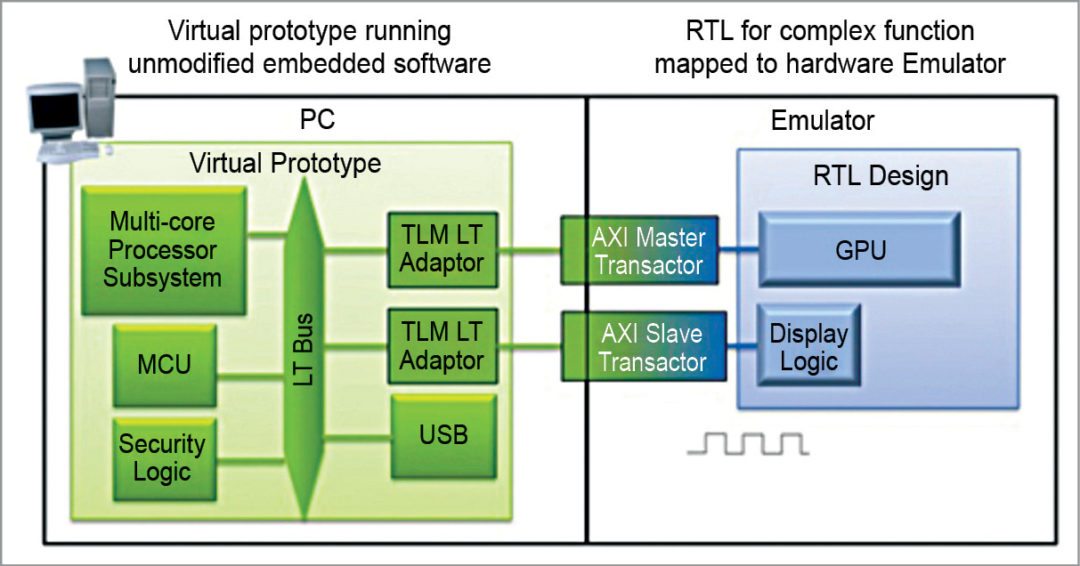
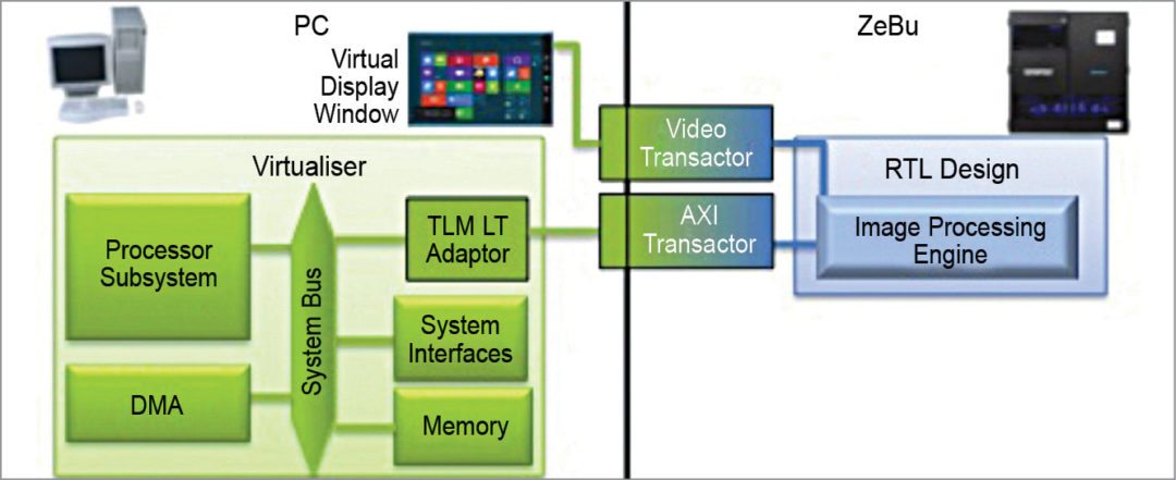
Hybrid emulation enables system on chip (SoC) development teams to take full advantage of their investments in a high-performance emulation system across their entire project to better meet increasing software, verification and competitive challenges. Typically, a model of the processor is run in the virtual platform and then the rest of the design is modelled by running the RTL on the emulator.

Virtual prototyping
Fig. 1: Virtual prototyping

Benefits of hybrid emulation

Hybrid emulation offers several benefits for SoC architecture, software and verification teams. For architects, it provides a mechanism to implement key elements of the SoC that are only available as RTL in a high-performance, cycle-accurate manner to support their architecture optimisation efforts. Users can choose cycle-accurate, approximately-timed or loosely-timed synchronisation between the virtual prototype and the emulator to make speed/accuracy tradeoffs.

Three main uses for hybrid emulation are architectural validation with accurate models, early software development and hardware verification.

In architectural validation with accurate models, high-speed models used to model processors are only functionally-accurate and not cycle-accurate, and you cannot get accurate performance or accurate performance data from these at that level of detail. Of course, you could just run the RTL of the processor on a simulator, but that is too slow.

In early software development, transactional-level models are often not available, are too low or do not exactly match the RTL for the block. But a hybrid approach with the processor in a virtual platform and all or most of the rest of the design in the emulator is fast enough for productive software development.

Hardware verification allows running actual software load.

Architectural validation.

For SoC architecture validation, you, as a user, have to link a high-performance emulator like ZeBu Server-3 to a virtual prototype exploration tool like Platform Architect MCO. ZeBu Server is the industry’s fastest emulation system. ZeBu solution includes ZeBu Server-3 emulator and a broad portfolio of ZeBu transactors, memory models and ZEMI-3 transactor compiler for rapid development of virtual system-level verification environments.

CPU clocks
Fig. 2: CPU clocks

ZeBu provides the comprehensive debug with full signal visibility and Verdi integration, and supports advanced use modes including power management verification and hybrid emulation with virtual prototypes for architecture optimisation and software development.
Platform Architect MCO enables system designers to explore and optimise the hardware-software partitioning and configuration of the SoC infrastructure, specifically the global interconnect and memory sub-system, to achieve the right system performance, power and cost.

Virtualiser
Fig. 3: Virtualiser

Using a high-performance emulator like ZeBu Server-3 with a virtual prototype exploration tool like Platform Architect MCO, testing typically consists of running application software tests on processor sub-systems in the emulator to drive simulation and monitoring performance. This confirms whether optimised configuration of the architecture design chosen during exploration meets the required performance metrics.

Verdi integration provides the powerful technology that helps comprehend complex and unfamiliar design behaviour, automate difficult and tedious debug processes and unify diverse and complicated design environments. ZeBu Server module emulates 60M gates in nine emulation chips. The components fit better, and fewer design nets get cut. It has less interconnect hardware. Highest performance is two to five megahertz, and it has low power, small size, gets latest processes every two years and is reliable.

Interconnect and memory sub-system peripherals are often modelled in Platform Architect MCO, with cycle-accurate CPU sub-systems modelled in ZeBu Server-3. In ZeBu world, various timing domains maintain their relative clock ratios. Operation in a fully-timed synchronisation mode provides full cycle accuracy. You can use this environment to run a variety of processing loads and data streams, and quickly analyse relative performance tradeoffs between various factors like cache sizes and number of processors. Typical results might show the impact on performance of variations in the number of data streams and processing loads.

Early software development and software-driven verification.

Hybrid emulation enables pre-silicon software development while part of the RTL design is still under development. It is also useful for system-level hardware-software co-verification. Virtual prototypes support the use of instruction-accurate SystemC/C++ processor models and other loosely-timed SystemC TLM-2.0 models. Such models remove the need to wait for silicon to begin developing or validating system software.

The post Hybrid Emulation And The Challenges Ahead appeared first on Electronics For You.


Smart System Controller for Nano Grids

$
0
0

An advanced approach has been developed to monitors and control small grid for better power utilization and fault detection. Power available at the grid which can come from multiple sources like solar, power plants, generators can be feed to the users intelligently. Depending upon the availability of power, it can be distributed priority wise among different types of users like hospitals, street lights, water pumps etc. All the related decision has been taken by a centralized control system called Multi Utility Controller. It not only includes operational controls but also energy measurement elements to analyze for better power distribution. Various parameters and usage information can be fetched using Power Line communication (PLC) from various smart utility meters like energy meter, gas meter, and water meter to generate bills and manage tariffs. The same controller can be used to communicate with street lights wirelessly for better usage and troubleshooting. This can help in saving power by controlling On/Off, light intensity remotely. All gathered information can be uploaded on server using LAN or GPRS connectivity for power analysis.

In developing countries like India, most of the population lives in small villages which have very limited availability of electricity or even does not have electricity at all. Smart Nano grids is the only solution to make them self-dependent for electricity and to face current challenges. These are digitally monitored energy systems that deliver electricity, water, gas from generation sources to points of consumption.

They optimize power delivery and facilitate two-way communication across the grid, enabling end-user energy management, minimizing power disruptions and transporting only the required amount of power. The result is a lower cost to the utility and the customer, more reliable power, and reduced carbon emissions.

Smart Nano Grid Architecture

Nanogrids are very small grids to serve a building or village with few number of houses with a typical load of 100 kW for grid-tied systems and 5 kW for remote systems not interconnected with a utility grid. In the current architecture, smart grid controller has been proposed which not only handles the power distribution but also control and monitor smart street lights. All the utility meters like energymeter, gas meter, water meter etc. are also connected with this controller for billing and other consumption analysis.


Annual Nano grid Revenues
Figure 1: Annual Nano grid Revenues

Smart Nano Grid Key Components

1. Multi Utility Controller
2. Load Dispatch Controller
3. Street Light Controller
4. Smart Utility Meters

Nano Grid Proposed Architecture
Figure 2: Nano Grid Proposed Architecture

Multi Utility Controller (MUC) is an adaptable controller system for a smart Nano-grid environment. It is a portable in size and battery operated so that utility worker can keep it along with him in the field. It has a LCD display to monitor the status of the grid and a user interface for grid control. Multiple type of communication protocol are available to communicate with different types of utility meters. All the gathered information is then uploaded on the server.

Multi Utility Controller Board
Figure 3: Multi Utility Controller Board

Load Dispatch Controller delivers power to different houses depending upon the power available. It has multiple relays to control the electricity delivery of each house. Status of all the houses and current power parameters like voltage, current has been sent to MUC using wireless communication. MUC analyze these parameters and sends command to load dispatch controller to control the distribution of available power.

Load Dispatch Controller Board
Figure 4: Load Dispatch Controller Board

Street Light Controller is a controller system for managing street lights using wireless communication. It is a battery operated system which takes its power from solar light for charging & then to run the LED light at night. It has the intelligence to monitor different system faults and then to send fault status to MUC.

Street Light Controller Board
Figure 5: Street Light Controller Board

Smart Utility Meters reads various usage information including total consumption parameters, instantaneous consumption, tariff-wise consumptions etc. along with configuring various parameters i.e. Configuration parameters, maintenance parameters, tamper management, tariff settings etc. sub–1GHz wireless communication or wired Power Line Communication helps meters communicate directly with MUC.

Smart Utility Meter
Figure 6: Smart Utility Meter

MUC System Architecture

MUC system has been designed around STM32F4 series microcontroller from STMicroelectronics. It is the high-performance ARM®Cortex-M4 32-bit RISC core operating at a frequency of up to 168 MHz suiting for this application. On chip 1 Mbyte Flash memory along with 192 Kbytes of SRAM met the memory requirements.

A 7.0 inch Amorphous-TFT-LCD (Thin Film Transistor Liquid Crystal Display) with a Resolution of 480(R.G.B) X 234 pixel is used to display the various parameters and to take the required inputs. MCU’s on Chip FSMC peripheral has been used to interface the LCD display.

The post Smart System Controller for Nano Grids appeared first on Electronics For You.

Development Kit that Realizes Cars to Generate and Express Their Own Emotions

$
0
0

TOKYO, July 19, 2017 ― Renesas Electronics Corporation (TSE:6723), a premier supplier of advanced semiconductor solutions, today announced that it has developed a development kit for its R-Car that takes advantage of “emotion engine” (Note 1), an artificial sensibility and intelligence technology pioneered by cocoro SB Corp., a SoftBank Group company. The new service kit enables cars with the sensibility to read the driver’s emotions and optimally respond to the driver’s needs based on their emotional state.

The service kit includes cocoro SB’s emotion engine, which was developed leveraging its sensibility technology to recognize emotional states such as confidence or uncertainty based on the speech of the driver. The car’s response to the driver’s emotional state is displayed by a new driver-concerning user interface (UI) implemented in the Renesas R-Car system-on-chip (SoC). Since it is possible for the car to understand the driver’s words and emotional state, it can provide the appropriate response that ensures optimal driver safety. As this technology is linked to artificial intelligence (AI) based machine learning, it is possible for the car to learn from conversations with the driver, enabling it to transform into a car that is capable of providing the best response to the driver. Renesas plans to release the development kit later this year.

Renesas will also demonstrate its connected car simulator incorporating the new development kit based on cocoro SB’s emotion engine at the SoftBank World 2017 event, to be held by SoftBank Corp. from July 20 to 21 at the Prince Park Tower Tokyo.

Renesas considers the driver’s emotional state, facial expression and eyesight direction as key information that combines with the driver’s vital signs to improve the car and driver interface, placing drivers closer to the era of self-driving cars. For example, if the car can recognize the driver is experiencing an uneasy emotional state, even if he or she has verbally accepted the switch to hands free autonomous-driving mode, it is possible for the car to ask the driver “would you prefer to continue driving and not switch to autonomous-driving mode for now?” Furthermore, understanding the driver’s emotions enables the car to control vehicle speed according to how the driver is feeling while driving at night in autonomous-driving mode. By providing carmakers and IT companies with the development kit that takes advantage of this emotion engine, Renesas hopes to expand the possibilities for this service model to the development of new interfaces between cars and drivers and other mobility markets that can take advantage of emotional state information.

Based on the newly-launched Renesas autonomyTM, a new advanced driving assistance systems (ADAS) and automated driving platform, Renesas enables a safe, secure, and convenient driving experience by providing next-generation solutions for connected cars.

Note 1: Emotion Engine, an artificial sensibility and intelligence technology, consists of two parts. The first part is voice emotion recognition that performs an analysis of a voice signal.
The second part is emotion generation technology that generates emotions for the device by forming a virtual hormone balance derived from various connected sensors. Then it makes it possible to perceive the speaker’s emotion by charting an “emotion map” as both a color, for example, yellow for happiness and red for sadness, and as volume level from 1-10.


The post Development Kit that Realizes Cars to Generate and Express Their Own Emotions appeared first on Electronics For You.

Single-Chip Buck-Boost Battery Charge Controllers Enabling USB Type-C and USB Power Delivery Support

$
0
0

New battery algorithm provides maximum input power for 1S to 4S applications

INDIA and DALLAS (July 20, 2017) – Texas Instruments (TI) (NASDAQ: TXN) today introduced a pair of highly flexible, single-chip buck-boost battery charge controllers for one- to four-cell (1S to 4S) designs. The bq25703A and bq25700A synchronous charge controllers support efficient charging through USB Type-C and other USB ports in end equipment ranging from notebooks and tablets to power banks, drones and smart home applications.

Supporting both I2C and SMBus interfaces, the bq25703Aand bq25700A feature a new advanced battery algorithm enabling full power output by adding intelligence to battery charging through maximum power point tracking technology. The unique algorithm, referred to as input current optimization (ICO), automatically detects the full capacity of input power to optimize current, while maintaining consistent system and charging current to ensure the utilization of maximum input power.

Key features and benefits

· Input source flexibility: The device’s USB Power Delivery compatibility offers an input voltage range from 3.5 V to 24 V, which designers can use in multiple ports including USB 2.0, USB 3.0 and the newest standard, USB Type-C.
· Wide USB On-the-Go (OTG) output compatibility: The new charge controllers support input-ready devices from 5 V to 20 V and adjustable output for USB OTG with programmable current regulation.
· Compact configurations: TI’s new battery-charging algorithm and intelligent detection features enable the battery charge controllers to support wide input and output voltage ranges and more compact adaptor designs.
· Seamless transition between different modes: The devices support 1S to 4S batteries and an efficient transition between buck and boost operation without any dead zone.

The bq25703A and bq25700A expand TI’s portfolio of industry-leading battery-charger solutions, offering switch-mode fast chargers and linear chargers for a broad variety of applications and power levels. Learn more about TI’s battery charging solutions for accurate, dependable and faster, cooler charging and how TI’s USB Type-C ecosystem provides protected power delivery for low power applications.

Tools and support

Designers can use the bq25700A evaluation module (EVM) to easily evaluate device features and performance and speed time to market. The bq25703A EVM and the bq25700A EVM are available from the TI store and authorized distributors for US$149.00. Designers can use the WEBENCH Battery Charger Designer to calculate the efficiency of the battery charge controller.


The post Single-Chip Buck-Boost Battery Charge Controllers Enabling USB Type-C and USB Power Delivery Support appeared first on Electronics For You.

Arduino Based Digital IC Tester Using MATLAB

$
0
0

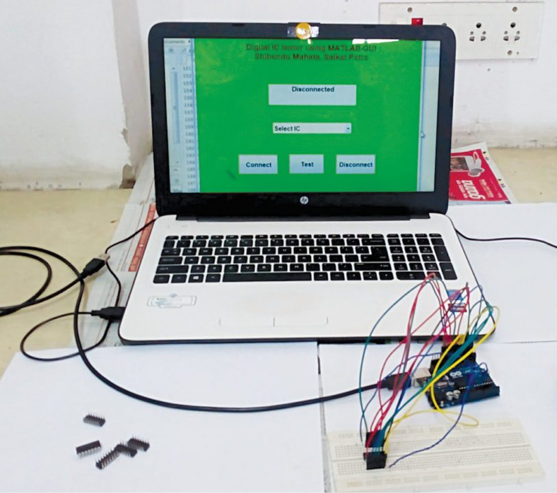
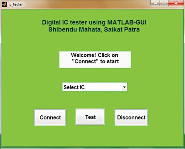
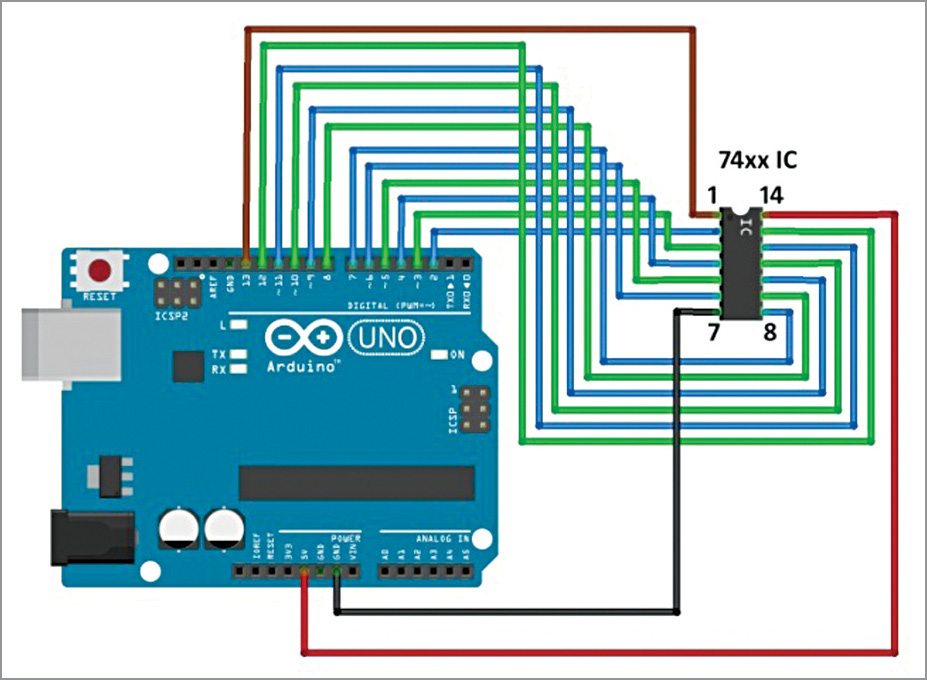
Testing of digital electronic systems generally involves applying a set of test stimuli to inputs of the device-under-test (DUT) and analysing responses of the system using a response analyser. If the DUT generates correct output responses (also called the golden response) for all the input stimuli, the DUT is regarded as fault-free. Those DUTs that fail to meet the golden response are regarded as faulty or defective. Block diagram for testing a device is shown in Fig. 1.

Block diagram for testing a device
Fig. 1: Block diagram for testing a device

This project describes testing of 74xx series digital ICs using a MATLAB graphical user interface (GUI) drop-down menu based approach. MATLAB acts as the test stimuli generator to the IC, which is the DUT. The GUI initiates communication with the Arduino and provides a user-friendly and interactive approach to conduct the test. The MATLAB source program (ic_tester.m) acts as the response analyser and displays test results on the front panel of the GUI.

Authors’ prototype of the Arduino-based digital IC tester and the MATLAB-based GUI front panel are shown in Figs 2 and 3, respectively.

Authors’ prototype of the digital IC tester
Fig. 2: Authors’ prototype of the digital IC tester
MATLAB-based GUI for testing the ICs
Fig. 3: MATLAB-based GUI for testing the ICs

Circuit and working

Circuit diagram of the Arduino-based digital IC tester is shown in Fig. 4.

Circuit diagram of the digital IC tester
Fig. 4: Circuit diagram of the digital IC tester

As mentioned earlier, MATLAB is used to apply stimuli to the DUT (74xx series digital ICs) and also record the response of the DUT to stimuli. It then compares the response of the DUT with the correct/golden response to test whether the device is faulty or not. For a digital IC, the correct response is given in the form of a truth table. Acting as a response analyser, the MATLAB verifies each and every possible outcome according to the truth table of a particular IC.

74xx series ICs that can be tested by this project are 7400, 7402, 7404, 7408, 7432 and 7486. Truth tables for these ICs are shown on the next page.

Software

1. Arduino IDE 1.6.5 is used to program the Arduino. The GUI application program has been developed in the R2014a version of MATLAB. The procedure to install the ‘Legacy MATLAB and Simulink Support for Arduino Package’ is described in ‘Controlling a Robotic Car Through MATLAB GUI’ DIY article.

2. After correctly setting up the path for the package, open source code files (ic_tester.m) of this project. Keep both the source code files in the same folder. Edit COM port (in the line a=arduino (‘COM19’)) with the port number in your PC where the Arduino Uno board has been installed. Run the file and click ‘Connect’ button to establish connection between MATLAB and Arduino Uno board. After successful communication is established, select proper IC from the drop-down menu and click ‘Test’ button in the GUI to test the IC.

Download source code


The post Arduino Based Digital IC Tester Using MATLAB appeared first on Electronics For You.

Harwin Launches SYCAMORE SMT Contact for Advanced Automated Assembly

$
0
0

Superior pin retention for modules and devices subject to multiple insertions and removals; patent-pending design; supplied on Tape & Reel

Portsmouth, UK, April 2017… Leading hi-rel connector and SMT board hardware manufacturer Harwin announces its new SYCAMORE surface-mount socket which provides superior pin retention and durability for high-volume applications manufactured using advanced automated systems. SYCAMORE’s design features three points of contact, providing the assurance of continuity and robustness previously only available from two-piece assemblies which are rarely available on Tape & Reel. Key markets for SYCAMORE include domestic and commercial gas detection systems, fire alarms and metering systems, plus many other applications which require modules and devices such as field-replaceable parts or temperature-sensitive components to be mounted to a PCB. SYCAMORE is a unique, proprietary Harwin contact design with patents pending.

SYCAMORE is a single-part SMT socket design featuring a low profile of only 0.3mm above the PCB. Available in top and bottom entry versions, it accepts 1.0mm or 1.50mm diameter pins and is open-ended, so mating pin depth is not limited. Manufactured from Beryllium copper, contacts are gold-plated to ensure high conductivity and durability over a temperature range of -50degC to +125degC.

“At Harwin, we understand the challenges of our customers right from design through to manufacturing and the unique contact design of our new SYCAMORE surface-mount socket addresses their need to apply advanced manufacturing processes for high volume output with no compromise on contact performance.” comments Robert Webber, Product Strategy Manager at Harwin.

SYCAMORE devices are available now, packaged on Tape & Reel, with 1400 parts per reel.

For more detail, please contact sales@harwinasia.com or visit our website www.harwinasia.com


The post Harwin Launches SYCAMORE SMT Contact for Advanced Automated Assembly appeared first on Electronics For You.

First SCR Thyristor Capable of Handling 600V 40Arms and 150°C Junction Temperature

$
0
0

Optimized for rectifier and phase control applications such as voltage regulators, heating and motor speed controls

Beijing, China, July 20, 2017 —Littelfuse, Inc., the global leader in circuit protection, today introduced a series of 40A standard high-temperature silicon-controlled rectifier (SCR) thyristors that are ideal for use as switches for rectifier and phase control applications such as voltage regulator, heating and motor speed controls. The new SJxx40x Series is the first SCR thyristor from Littelfuse capable of handling 600V, 40Arms and junction temperatures up to 150°C.

SJxx40x Series SCR Thyristor

The SJxx40x Series is designed to prevent the overheating and thermal runaway problems SCRs can experience due to an application’s limited cooling capability or occasional overload situation. They are designed to trigger with just a few milli-amps of current at less than 1.5V potential.

Typical applications for SJxx40x Series SCR Thyristors are rectifiers in a variety of end uses including AC solid-state switches, industrial power tools, exercise equipment, white goods and commercial appliances.

“Designers who once had to deal with limited cooling capabilities can now take advantage of an SCR Thyristor with the ability to operate at higher temperatures, which minimizes the risk of an uncontrolled temperature increase in challenging applications,” said Koichiro Yoshimoto, business development manager at Littelfuse. “Switching to the new SJxx40x Series will make it possible to handle more current or use a smaller heat sink to handle the same power.”

SJxx40x Series SCR Thyristors offer these key benefits:
• Capable of handling high load current and occasional overloads under limited cooling conditions due to high junction temperature (TJ) of 150°C.
• Available in both TO-220AB and TO-263 packages to support flexible mounting options for easier device design.
• High on-state current (IT) of 40Arms allows the SJxx40X to handle higher load currents.
• High rate of voltage change over time (dv/dt) enables the SJxx40X to tolerate more line noise and surge often found in commercial AC lines.


The post First SCR Thyristor Capable of Handling 600V 40Arms and 150°C Junction Temperature appeared first on Electronics For You.

Real Time Face Recognition Using Python And OpenCV

$
0
0

A real time face recognition system is capable of identifying or verifying a person from a video frame. To recognize the face in a frame, first you need to detect whether the face is present in the frame. If it is present, mark it as a region of interest (ROI), extract the ROI and process it for facial recognition.

Real time face recognition software

This project is divided into two parts: creating a database, and training and testing.

Creating a database.

Take pictures of the person for face recognition after running create_database.py script. It automatically creates Train folder in Database folder containing the face to be recognised. You can change the name from Train to the person’s name.

While creating the database, the face images must have different expressions, which is why a 0.38-second delay is given in the code for creating the data set. In this example, we take about 45 pictures/images and extract the face, convert it into gray scale and save it to the database folder with its name.

Training and testing.

Training and face recognition is done next. face_rec.py code does everything. The algorithm used here is Local Binary Patterns Histograms (LBPH).

Screenshot of Haar features
Fig. 1: Screenshot of Haar features

Face detection is the process of finding or locating one or more human faces in a frame or image. Haar-like feature algorithm by Viola and Jones is used for face detection. In Haar features, all human faces share some common properties. These regularities may be matched using Haar features, as shown in Fig. 1.

Two properties common to human faces are:
1. The eye region is darker than the upper cheeks.
2. The nose bridge region is brighter than the eyes.

Composition of two properties forming matchable facial features are:
1. Location and size including eyes, mouth and bridge of nose
2. Value for oriented gradients of pixel intensities.

For example, the difference in brightness between white and black rectangles over a specific area is given by:

Value = Σ (pixels in black area)- Σ (pixels in white area)

The above-mentioned four features matched by Haar algorithm are compared in the image of a face shown on the left of Fig. 1.

Testing procedure

Install OpenCV and Python on Ubuntu 16.04.

The project was tested on Ubuntu 16.04 using OpenCV 2.4.10. The following shell script installs all dependencies required for OpenCV and also install OpenCV 2.4.10.

$ sh ./install-opencv.sh

After installing OpenCV, check it in the terminal using import command, as shown in Fig. 2.

Checking OpenCV using import command
Fig. 2: Checking OpenCV using import command
Creating the database
Fig. 3: Creating the database

1. Create the database and run the recogniser script, as given below (also shown in Fig. 3). Make at least two data sets in the database.

$ python create_database.py person_name

2. Run the recogniser script, as given below:
$ python face_rec.py

This will start the training, and the camera will open up, as shown in Fig. 4. Accuracy depends on the number of data sets as well as the quality and lighting conditions.

 Screenshot of face detection
Fig. 4: Screenshot of face detection

OpenCV 2.4.10.

OpenCV provides the following three face recognisers:
1. Eigenface recogniser
2. Fisherface recogniser
3. LBPH face recogniser

In this project, LBPH face recognition is used, which is createLBPHFaceRecognizer( ) function.

LBP works on gray-scale images. For every pixel in a gray-scale image, a neighbourhood is selected around the current pixel and LBP value is calculated for the pixel using the neighbourhood.

After calculating LBP value of the current pixel, the corresponding pixel location is updated in the LBP mask (it is of same height and width as input image.) with LBP value calculated, as shown in Fig. 5.

Screenshot of a LBPH face recogniser
Fig. 5: Screenshot of a LBPH face recogniser

In the image, there are eight neighbouring pixels. If the current pixel value is greater than or equal to the neighbouring pixel value, the corresponding bit in the binary array is set to 1. But if the current pixel value is less than the neighbouring pixel value, the corresponding bit in the binary array is set to 0.

Download source code


Interested in face detection projects? Check out face recognition using Raspberry Pi.

The post Real Time Face Recognition Using Python And OpenCV appeared first on Electronics For You.


‘India Innovation Challenge 2017’ to nurture engineering innovation among university students in India

$
0
0

Collaboration with IIM Bangalore and the Department of Science and Technology will mentor students and fund winning teams with INR 3.5 crore for start-up
India, Bangalore, July 21, 2017: Texas Instruments (TI) today announced the launch of the second edition of India Innovation Challenge Design Contest (IICDC 2017), with registrations for the contest opening on July 20th, 2017 at www.ti.com/iicdc. The last date for registration is September 10, 2017. will be TI will continue the collaboration with the Indian Institute of Management Bangalore (IIMB) and Department of Science and Technology (DST) to nurture innovation and consistent with the goals of the Make in India program. In the year long journey, IICDC 2017 will include an intense mentoring program for students.

Last year, IICDC 2016 attracted registrations from 11,000 engineering students across 624 colleges in India. Anamika Verma, an IIT Mumbai participant, said: “IICDC has raised standards for other design contests in the country. TI, along with its partners, worked with us as a team. I would highly recommend students from engineering colleges to apply for IICDC 2017.”

During IICDC 2017, TI will provide resources and in-depth technical training program throughout the contest. DST will provide INR 3.5 crores to the student start-ups for prototyping and seed funding. NSRCEL at IIM Bangalore will provide business mentoring and incubation support. MyGov, the government’s online portal, will be extended to the participants for registration.

“TI believes in nurturing engineering students through our university program, especially through experiential learning. IICDC is a great example of this. We are thankful to all the partners for helping us build IICDC as a thriving platform for young minds to generate ideas and then launch their start-ups.” said, Sanjay Srivastava, Director, TI India University Program.

Professor Suresh Bhagavatula, Chairperson, Entrepreneurial Ecosystem Development, NS Raghavan Centre for Entrepreneurial Learning (NSRCEL) at IIM Bangalore, said: “IIMB sees an exciting opportunity through this collaboration with TI on the IICDC by coming across unique entrepreneurial ideas from the best talents of the country and helping them incubate the ideas and transform them into successful enterprises. With mentors from NSRCEL, we see a lot of growth and competitive opportunity for students who want to address critical problems through their innovations.”

“DST’s collaboration with TI’s IICDC provides impetus to the development of science and technology within the country. With this, we encourage students to engineer path-breaking solutions that bring socio economic change.” said Mr. H.K. Mittal, advisor and head of NSTEDB, DST.

Commenting on the partnership, Mr. Gaurav Dwivedi, CEO of MyGov, said: “MyGov is glad to support DST and TI India in bringing innovative ideas from different corners of the country to one platform, thus further strengthening government’s Make in India program. The Innovative Platform of MyGov has been developed by National Informatics Centre (NIC) that has great engagement and evaluation features to conduct such contests. The platform has hosted number of such innovative contests in recent years.”


The post ‘India Innovation Challenge 2017’ to nurture engineering innovation among university students in India appeared first on Electronics For You.

Controlling A Linear Actuator With An Arduino

$
0
0

There is a wide application of linear actuator where one wants to move something but they do not want to physically get involved in moving it. There are quite a number of ways to control linear actuators depending on the application and the user experience required. These are the key aspects determining the setup and the way this setup will operate. It is common for most movements to involve manual control using remote control or a rocker switch. It is however paramount, that the system has some form of intelligence to improve the level of efficiency involved.

Microcontrollers, and relays in some cases are required for the intelligence in the system setup. Here we use an Arduino, a popular microcontroller board that provides an ease of setting up. There are other alternatives, but Arduino has a lower learning curve.

Controlling linear actuator using Arduino
Controlling Linear Actuator using Arduino

The parts required for the project setup are Arduino UNO, progressive automation PA-14-6-50, 12V 5A power supply, female power plug, small flat head screwdriver, pololu VNH5019 motor driver rated at 12v5a and SPDT relays. These are easily available, and are part of a setup that is easy to build and comes up with a powerful automated system.

Progressive
Actuator

In reference to the linear actuator circuit assembly, the board comes with male headers and screw terminals unattached. This can be attached through a soldering iron. There are four holes on the board which are considerably large. These are for the wires which are not the right spacing, considering the screw terminals. However, there are a pair of smaller holes which are the right fit.. The female power plug is then screwed onto the GND/VIN on the VNH5019. This allows easy plugging and unplugging the power supply. It is also possible to put switch to facilitate for an E-stop.

Arduino is powered via a USB. It is also possible to have a 12v5a power as well as the USB. It is important to note that the Arduino can handle 12V power, so one can get the 12v6a power supply and still power everything using the USB.

Software

There is software required to automate the functions of the setup.The first part includes making sure that the Arduino pins that trigger the relays are set to outputs.

//Use constants for the relay pins in case you need to change these later
const int relay1 = 6; //Arduino pin that triggers relay #1
const int relay2 = 7; //Arduino pin that triggers relay #2

void setup() {
//Set pinMode to OUTPUT for the two relay pins
pinMode(relay1, OUTPUT);
pinMode(relay2, OUTPUT);

}

void extendActuator() {
digitalWrite(relay1, HIGH);
digitalWrite(relay2, LOW);
}

It is crucial to test if the setup is working. In the code below, the actuator is set to extend for one second, stop for one second, retract for one second and the pause for five seconds, before repeating the process.

void retractActuator() {
digitalWrite(relay1, LOW);
digitalWrite(relay2, HIGH);
}

void stopActuator() {
digitalWrite(relay1, LOW);
digitalWrite(relay2, LOW);

void loop() {
extendActuator();
delay(1000);

stopActuator();
delay(1000);
retractActuator();
delay(1000);

stopActuator();
delay(5000);

/Use constants for the relay pins in case you need to change these later
const int relay1 = 7; //Arduino pin that triggers relay #1
const int relay2 = 6; //Arduino pin that triggers relay #2


Feel interested? More articles available on the circuits page.

The post Controlling A Linear Actuator With An Arduino appeared first on Electronics For You.

Learning Corner: Arduino Timers

$
0
0

In this video, the presenter will show you how to use the timer of a microcontroller (Arduino Uno — ATmega328P) to not only create precisely timed events but also generate a PWM signal with variable duty cycle and frequency up to 8MHz.

Courtesy: GreatScott!


The post Learning Corner: Arduino Timers appeared first on Electronics For You.

6 Awesome Innovations for Techies

$
0
0

Presented here are 6 awesome innovations from the tech world. Let us know which one you would like to get your hands on.

Transform any laptop screen into a touchscreen

Price, glare and battery drain are three reasons that could discourage you from buying a touchscreen laptop. Neonode has developed a simple but innovative USB-powered device that can transform any ordinary laptop into a touchscreen one at a fraction of the cost.

A CES 2017 Innovation Awards Honouree, AirBar is a sleek matte-finished strip that attaches to the bottom of your laptop screen using magnets, and plugs into the nearest USB port. That’s it—no calibration or software installation required. Now, AirBar starts projecting an invisible light field on the surface of your display that makes it possible to use it like a touchscreen. You can interact with your laptop using Windows gestures like pinch, swipe, zoom and scroll. Unlike regular touchscreen laptops, you can use AirBar ‘touchscreen’ with anything—bare hands, gloved hands, a pen, a paintbrush, stylus or whatever. This is because the light field reacts to any disturbance without requiring any minimal touch activation force.

AirBar does away with glare too. Light transmission is 100 per cent as nothing is built atop or inside your screen. There is just an invisible light field being emitted from the bar.

AirBar comes in three different sizes to suit different screen sizes: 33.8cm (13.3-inch), 35.6cm (14-inch) and 39.6cm (15.6-inch). It works on all Windows 10 laptops. There is also a version compatible with MacBook Air 33.8cm. Currently, AirBar does not work with some devices like MacBook Pro because it requires at least 17mm of space below the display to snap on. However, the company has just revealed to EFY that they are planning to expand their suite of products to fit additional laptops such as MacBook Pro.

Company: Neonode; Country: Stockholm, Sweden; Website: www.air.bar

AirBar is a discreet device that fits below your laptop display and transforms it into a touchscreen

The post 6 Awesome Innovations for Techies appeared first on Electronics For You.

Cyberattacks | Healthcare Security | Remote IoT Devices

$
0
0

27,482 Cyber Security Incidents Reported in H1 2017

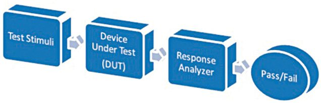
Over 27,000 cyber security incidents were reported in the first six months of this year to Indian Computer Emergency Response Team (CERT-In), Parliament was informed today. These incidents include phishing, website intrusions and defacements as well as ransomware attacks. The government has also formulated Crisis Management Plan for countering cyberattacks and cyber-terrorism for implementation by all ministries/departments of Central government, state government and their organisations and critical sectors.

Besides, cyber security mock drills are being conducted regularly to enable assessment of cyber security posture and preparedness of organisations in the government and critical sectors, including corporate sector. The minister said 15 such drills have so far been conducted by CERT-In, where 148 organisations from different states and sectors such as finance, defence, power, telecom, transport, energy, space, IT/ITeS etc participated. (Read More)


“Scary” number of Healthcare IT Execs put Faith in Inadequate IoT Security

More than 70 percent of healthcare IT decision makers (ITDMs) believe that traditional security products can secure IoT-Connected medical devices. That’s according to a survey of 200 healthcare ITDMs by IT security company Zingbox, fielded earlier this month.

The survey found that more than 90 percent of healthcare IT networks have IoT devices – such as infusion pumps or glucometers – connected to them.

The large majority of the IT decision makers surveyed believe that the same products used to secure laptops and servers are sufficient to secure IoT-connected medical devices. They also believe that the same technologies can detect irregularities in network traffic. In addition, 76 percent of healthcare ITDMs said they were confident or very confident that all devices connected to their network are protected. (Read More)


Bad Code Library Triggers Devil’s Ivy Vulnerability in Millions of IoT Devices

Tens of millions of products ranging from airport surveillance cameras, sensors, networking equipment and IoT devices are vulnerable to a flaw that allows attackers to remotely gain control over devices or crash them.

The vulnerability, dubbed Devil’s Ivy, was identified by researchers at Scenario, who singled out high-end security cameras manufactured by Axis Communications. Scenario said 249 models of 251 Axis cameras are vulnerable to unauthenticated remote attackers who can intercept a video feed, reboot cameras, or pause a video feed while conducting a crime.Researchers said Axis Communications isn’t alone, reporting 34 companies use the same underlying flawed software; including Microsoft, IBM, Xerox and Adobe. Those companies are part of the ONVIF Forum, an unofficial international consortium of hardware vendors. (Read More)


The post Cyberattacks | Healthcare Security | Remote IoT Devices appeared first on Electronics For You.

Want to Build an Electronic Device Based Business? Incubation Centre IIT Patna Can Can Help You

$
0
0

There is a long way between an innovative product idea and a market-ready product.
An electronic product, with its circuitry, peripherals, power supply, display and enclosure is a complex machine. Unlike software platforms, where interim versions are easier to produce, test and deploy into production systems, an electronic device needs to be thoroughly designed, tested and proved before being put into manufacturing and market.

This makes prototyping and testing of your product for the intended use is very critical. It has to go through design, engineering, then prototyping and finally manufacturing.

While designing any new electronic product, simulation and design on EDA software can be quite useful. It is not easy for a startup company to acquire the tools necessary for doing this, as most of the industry grade software used for this purpose are highly expensive.

Incubation Centre IIT Patna has set up a state of the art design laboratory where these facilities are available to an incubated startups.

In certain conditions, verification in real world becomes necessary. Performing electronic prototyping got several advantages because it allows to validate electronic hardware for

  • Components compatibility between each other so as to ensure that the PCBA will work properly.
  • Engineering of the board: As components being tested in real situation, it allows us to determinate if the board is designed to specification and how it will operate in situations similar to actual use.
  • Pre-certify the board: As our PCBA is assembled and almost as similar than your future production one, we can perform pre-certification with our PCBA prototype against different standard
  • Pre-certify the board: As our PCBA is assembled and almost as similar than your future production one, we can perform pre-certification with our PCBA prototype against different standard
  • Validate mechanical constraints like Spacing and interference
  • Validate thermal constraints like Heat dissipation

Incubation Centre IIT Patna has set up prototyping and testing laboratories with state of the art equipment for PCBA and final product creation.


The post Want to Build an Electronic Device Based Business? Incubation Centre IIT Patna Can Can Help You appeared first on Electronics For You.

DC Power Distribution: Need To Think Of Current Situation

$
0
0

In India, electrical distribution infrastructure is not well extended in rural areas. However, with advanced development in power electronics switching and control devices, it is now possible to replace an existing AC power distribution network with a DC power supply for better energy efficiency. For this, a case study of actual load data has been done at academic buildings of Matoshri College of Engineering, Nashik. Energy-efficiency analysis on different loads has shown that, if an existing AC power distribution network is replaced by a DC distribution network, considerable amount of energy can be saved.

Current scenario

The electrical power distribution system at the end of 19th century was based on DC technology. This Edison DC distribution system had the disadvantage that power-generating plants feeding heavy distribution conductors and consumer loads tapped of these. This system operated at the same voltage level throughout.

But to have a better option, a three-wire system was also used to save the cost of the copper conductor. The three wires were at 110, zero and -110 volts relative potential. 100-volt lamps could be operated between either +100 or -100-volt legs of the system and zero-volt neutral conductor that carried only unbalanced current between the positive and negative sources.

For fast-growing power electronics development, it is possible to completely replace the existing AC distribution network with DC distribution network, from the point of view of today’s power system scenario at distribution side. Most of the loads on distribution side are of DC type and, unfortunately, these all are fed by an AC-type supply distribution system involving a number of energy-conversion stages.

In case of AC type there should be source synchronisation, which is not required in case of DC. DC can be drawn directly from solar, wind and the grid by the loads, depending on which source is available. Harmonic issues and phase-balancing problems are not present in a DC system. It offers a lower cost of ownership in building wiring, copper and connectors along with an increase in efficiency of eight to ten per cent, which is truly significant.

A proper distribution system offers higher efficiency and the potential to extract power from multiple available sources. Then there are benefits that are not as immediately apparent. Most back-up energy sources such as batteries and flywheels are inherently DC.

Further, telecom and server loads run on DC, so there are fewer intermediate efficiency-robbing stages, along with greater reliability due to fewer potential points of failure with the DC approach. According to Central Electricity Authority (CEA), India has a shortage of around 11 per cent peak demand and more than 24 per cent T&D losses. In most rural areas, electricity is not available for more than eight hours a day, so it is necessary to move towards energy-efficient techniques with renewable energy support.

Low-voltage DC distribution system topologies

A low-voltage DC (LVDC) system is of two types, accordingly to conductor polarities:

Unipolar LVDC system.

In this type of distribution system, voltage level throughout the system is the same. The two-conductor system has one conductor at positive polarity and another at zero or neutral polarity. Entire load on the distribution system is connected at this voltage level, as shown in Fig. 1.

A unipolar LVDC distribution system
Fig. 1: A unipolar LVDC distribution system

Bipolar LVDC system.

A bipolar LVDC system is a combination of two series-connected unipolar systems. In this system, it is the choice of the customer to connect to the appropriate voltage level. The choices are:
1. Positive to neutral polarity
2. Negative to neutral polarity
3. Positive to negative polarity
4. Positive to negative polarity with neutral connection

Fig. 2 shows the possible alternatives for a consumer connection. Customer connections 1 and 2 can lead to an unsymmetrical loading situation between DC poles in the system. Possible over-voltage can be restricted with a cable cross-section selection. Connections 1 and 2 are used in studied ±750V DC bipolar system. Main lines of the system contain all three conductors but customer connections have two-wire cables connected between positive or negative poles. Therefore customer supply voltage is either +750V DC or -750V DC.

Bipolar LVDC distribution system with different customer connection alternatives
Fig. 2: Bipolar LVDC distribution system with different customer connection alternatives

Energy efficiency analysis of AC/DC, DC/DC and DC/AC conversions

According to the survey of different products in the market, some conversion efficiencies for different wattage ratings are given in Table I, which can be further used for calculations.

Losses calculation

Loads in the building.

Academic buildings consist of different connected loads, broadly mentioned in Table II with their wattage ratings. From Table I it is clear that, according to the wattage rating, conversion efficiency of every electrical equipment is different. Now, to calculate the total energy consumed by each equipment, a site survey was done. According to the site survey, total electricity consumed by a particular load is given in Table II.
<1–nextpage–>

Power supplies of loads in the building.

From the above-mentioned data of connected loads for the buildings, conversion efficiency formulae for different loads are given as follows:

Desktop computers.

Efficiency for desktop computers on existing AC supply is given by:
ηAC= ηUPS×ηT×ηAC/DC×ηDC/DC×ηFeeder …….. (1)

If the same is used to supply from DC power system, power efficiency is:
ηDC= ηUPS×ηDC/DC×ηFeeder …….. (2)

where ηUPS is the power efficiency of UPS (75 per cent taken here by measurement), ηT is the power efficiency of transformer, ηAC/DC is the power efficiency of AC/DC, ηDC/DC is the power efficiency of DC/DC and ηFeeder is the power efficiency of feeder, which is 100 per cent.

Other loads.

Like desktop computers, it is possible to calculate the power conversion efficiency for AC and DC supply for all other loads.

For fluorescent lamps:
ηAC= ηFeeder …….. (3)
ηDC= ηDC/DC×ηFeeder …….. (4)

For printers and IT devices, these efficiencies are calculated using equations (1) and (2).

For LED lights and photocopy machines:
ηAC= ηAC/DC×ηDC/DC×ηFeeder …….. (5)
ηDC= ηDC/DC×ηFeeder …….. (6)

Similarly, power efficiencies can be calculated for all the loads, and their calculated values are summarised in Table III.

It is clear from the above analysis that in a distribution system, where most loads are of DC type, a DC distribution system works quite efficiently. Also, effective energy saving of 18 per cent is possible.

Calculations for energy-conversion efficiency of a building have been established for various loads. During the conversion from AC/DC, DC/AC and DC/DC, power losses are calculated with efficiency for AC and DC supply with proper comparison.

Compared to an AC distribution system, a DC distribution system has 18 per cent more efficiency. Thus, a DC distribution system with bipolar DC feeder has a great future in India to achieve Late Dr A.P.J. Abdul Kalam’s Vision of 2020.


The post DC Power Distribution: Need To Think Of Current Situation appeared first on Electronics For You.


SnapEDA: New parts library for PADS & DX Designer accelerates PCB design

$
0
0

Designers can build circuit boards faster with millions of symbols & footprints on SnapEDA

July 18, 2017 – SAN FRANCISCO – Mentor, a Siemens business, and SnapEDA, the Internet’s first parts library for circuit board design, are announcing new support for Mentor PADS and DX Designer on SnapEDA.

Whether building satellites or medical devices, hardware designers spend days creating digital models for each component on their circuit boards, a painful and time-consuming process that hinders product development.

With today’s launch, Mentor PADS & DX Designer customers will gain access to SnapEDA’s extensive component library containing millions of symbols, footprints, and 3D models, further enhancing the vast resources available for Mentor PCB design software.

All parts are auto-verified with SnapEDA’s proprietary verification technology, helping to reduce risk and unneeded, costly prototype iterations. This technology answers common questions designers have about libraries, such as “what standards does this footprint conform to?”

As the world becomes more connected, electronic devices are proliferating and diversifying, and time-to-market is more crucial than ever for companies to stay competitive.

“We’re seeing a shift in the industry where it’s no longer just large enterprises designing electronic products. Today, mid-size companies, startups, and even non-traditional companies, such as apparel companies, are making printed circuit boards,” said Natasha Baker, founder & CEO of SnapEDA.

“The challenge they face is that – unlike large enterprises – they often don’t have dedicated librarians helping with parts creation. This means they’re spending valuable time creating parts from scratch. By making our library available for PADS & DX Designer, we’re empowering designers to spend more time with the powerful functionality in these tools, enabling them to build better products in less time.”

The PADS Product Creation platform is targeted for individuals and small teams who are designing electronics systems. The PADS solution provides users with an easy to use, affordable, and highly integrated platform for design entry, PCB layout, circuit simulation and electrical and thermal analysis capabilities, enabling higher design productivity, enhanced product quality, and cost and design cycle reduction. It builds on the strong PADS legacy – production-proven on millions of designs by hundreds of thousands of engineers worldwide.

“We are beginning to see a new breed of design engineer – those who do it all with a focus on the complete end product”, said Paul Musto, Marketing Director for the Board Systems Division of Mentor, a Siemens Business. “These individuals are attempting to navigate the many disciplines of design, e.g. mechanical, electrical, software, and are encumbered with the creation of so many different parts and libraries. SnapEDA’s solution for providing electronic libraries through an open forum is a huge time and energy saver for this community of engineers. Mentor, a Siemens business, is pleased to partner with SnapEDA to help this community become more efficient and allow them to focus on their end product rather than spending cycles creating libraries.”

About SnapEDA

SnapEDA is the Internet’s first & leading parts library for circuit board design. By providing blueprints for circuit board design via our website and within PCB design tools, we shave days off product development and reduce the risk of production delays, so that designers can focus on product optimization and innovation. Thousands of hardware designers worldwide rely on SnapEDA to design faster, whether they’re making smartwatches, drones or robots. The company is funded by Y Combinator and private investors. Visit www.snapeda.com to learn more.


The post SnapEDA: New parts library for PADS & DX Designer accelerates PCB design appeared first on Electronics For You.

SNUG India Celebrates 18th Year With Record Gathering of Semiconductor Design Community

$
0
0

Dr. Aart de Geus, Synopsys Chairman and Co-CEO, Kicked off the Annual Two-Day User Event

Bangalore, July 17, 2017 – Synopsys, Inc. (Nasdaq: SNPS) today announced that it has hosted its 18th annual Synopsys Users Group (SNUG) conference in India to help engineers better address the productivity challenges they face when designing chips and electronic systems. The conference has become the industry’s premier gathering of semiconductor professionals in India. Synopsys tool, IP and software users attended the two-day conference on July 12th and 13th at the Leela Palace in Bangalore. Launched in 2000, SNUG India is part of a global program that began in 1991 and currently includes 15 user conferences worldwide with more than 10,000 participants annually.

SNUG India 2017 featured user papers plus presentations on design synthesis, low-power implementation and verification, test, mixed-signal verification, IP integration, emulation, virtual prototyping, FPGA-based prototyping. This user-driven event promotes strong engagement among semiconductor professionals and provides a platform for sharing best practices and methodologies in semiconductor design. SNUG worldwide is driven by its mission to enable designers to learn, interact and participate. This year’s event featured new electronic design automation (EDA) solutions and design techniques for physical implementation, verification, custom design and IP to meet the immense challenges posed by designing semiconductor electronics at 7nm and below.

In his opening keynote address, Dr. Aart de Geus, chairman and co-chief executive officer at Synopsys, spoke about “silicon to software to smart everything” becoming the stimulus that is driving the next wave of innovation. He described Synopsys’ unique ability to partner with the semiconductor industry in the quest to produce innovative future designs especially in the age of digital intelligence.

“After computation for 20 years and mobility for 15 years, we are now entering the era of digital intelligence. Digital intelligence will massively change the world, and we are in the midst of this. It changes the world in every possible aspect that you can think of. Wearables, things in your home, your car―everything will be touched,” said Dr. de Geus.

Dr. Pradip K. Dutta, group vice president and managing director of Synopsys India and Sri Lanka, said, “SNUG has become the leading forum for the electronic design engineering community to connect with each other, and to interact with Synopsys executives and technologists. This year we had pioneering keynotes from our chairman and co-CEO as well as from our partner, STMicroelectronics, on why digital intelligence matters and why semiconductors will play a pivotal role in digital era.”

In his keynote address on “Sand to Cloud: Can India Ride ‘Smart X’ Wave,” Vivek Sharma, managing director at STMicroelectronics, spoke about accelerating the momentum of making almost everything smarter while bringing together the diverse players of our vast ecosystem in an unprecedented way. “Semiconductors today play a pivotal role across various verticals like smart driving, smart industry, smart cities and homes. India has a huge opportunity to play in the digital era and make the most of the smart wave.”

A conference of this breadth would not be successful without industry ecosystem participation. SNUG India 2017 Platinum Sponsors are ARM, GLOBALFOUNDRIES, Samsung and TSMC.


The post SNUG India Celebrates 18th Year With Record Gathering of Semiconductor Design Community appeared first on Electronics For You.

INNOVATION on Agriculture Farms Wins Chairman’s Award

$
0
0

· 10 student teams receives 2 Crore funding from DST to launch their start-up company and incubated at NSRCEL, IIMB

Bangalore, July 22, 2017: Sri Ramakrishna Institute of Technology College, Coimbatore bagged Chairman’s Award for the best innovative product for the Texas Instruments India Innovation Challenge Design Contest 2016. This was announced at the grand finale held at IIM Bangalore and was presided by top minds in academia and industry. The dignitaries present were Prof. Ashok Jhunjhunwala, Shri NS Raghavan, Shri Harkesh Kumar Mittal, Dr. Anita Gupta, Prof. G Raghuram, Dr. Peter Balyta and Sanjay Srivastava.

The first runner up for the Texas Instruments IICDC 2016 is the team from IIT Kharagpur for their innovation on tracking sleep disorder and the second runner up is from Dream Institute of Technology, West Bengal for their innovative solution on safety ensuring wearable. Total 30 teams participated in the finals which received 1.5 crores as product development fund. Out of these, Jury selected 10 teams which will receive INR 2Crores seed fund and opportunity to be incubated at NSRCEL, IIMB.

The 2016 TI IICDC saw participation from ~11,000 engineering students across 624 colleges in India. The collaboration with Indian Institute of Management Bangalore (IIMB) and Department of Science and Technology (DST) has helped to nurture the young engineering minds and support the Make in India Program at IICDC 2016. In the 10 months long challenge, the participants saw an intense mentoring program from IIMB and TI. TI provided technical resources and guidance throughout the contest, including tool support and mentoring to design & help the students make their prototypes. DST provided funding of INR 3.5 crores to the student start-ups, which went towards the product development and seed fund. The online platform MyGov, promoted active participation of Indian citizens in the country’s governance and development, helped students from all different corners of the country to register for the IICDC through the MyGov portal.

Commenting on the award ceremony, Mr. Laxmi Kant Tiwari from IIT Kharagpur, one of the selected 10 teams said, “We feel honoured and privileged to emerge winners of this year long challenge. It feels all the more exciting to know that we competed amongst the best minds in the country and we were chosen by eminent jury members as the winning idea.

We are confident that we will be able to work on this innovation further with the assistance and guidance from TI, IIM B and our mentors. We are all thrilled to start our new journey as entrepreneurs”


The post INNOVATION on Agriculture Farms Wins Chairman’s Award appeared first on Electronics For You.

Countdown Timer

$
0
0

Sometimes there is a need to switch on or off electrical appliances or gadgets after a predetermined time. The circuit presented here can switch on/off any electrical appliance (load) through a relay switch after the specified time set in minutes or seconds.

The timer can be easily set with four switches (S3 through S6) to select minutes/seconds, hundredths, tenths and units. Two more switches are used to start (S2) and stop (S1) the timer.

Circuit and working

Circuit diagram of the countdown timer is shown in Fig. 1. ATmega8A (IC1) from Atmel is at the heart of the circuit. Associated components include a 16×2 liquid crystal display (LCD1), two BC547 transistors (T1 and T2), a piezobuzzer (PZ1), a 12V single-changeover (1C/O) relay and a few other components.

Circuit diagram of countdown timer
Fig. 1: Circuit diagram of countdown timer

The system works in three modes: started, stopped and setting. Started means the countdown is under process and settings are not allowed. Stopped means the countdown has stopped and the user can change settings to start the countdown timer afresh. In setting mode, the input switches (S3 through S6) are enabled for countdown timer settings.

When start switch (S2) is pressed, relay RL1 energises and the countdown starts. The timer stops automatically when the countdown reaches 000 or stop button (S1) is pressed. The status of countdown is shown on LCD1. A beep is generated by the piezobuzzer when the countdown reaches below ten seconds and stops when the countdown reaches 000. Jumper J1 can be disconnected if the buzzer is not required. The power supply to relay RL1 depends on the coil voltage of the relay (like 5V, 6V or 12V). Here, we used 12V DC at CON1 for the relay.

In stopped or setting mode, LED1 blinks every ten seconds. When start (S2) button is pressed, LED1 blinks every second.

Software

The software is written in ‘C’ language and compiled using an AVR Studio 4 software. You can use any suitable software to burn the hex code into the microcontroller through ISP port. At EFY Lab, we used ProgISP programmer for the purpose.

Before programming, set fuse bits for the 3.6864MHz crystal option as shown in Fig. 2.

Screenshot of the fuse bits settings; ‘1’ means ‘unprogrammed’ and ‘0’ means ‘programmed’
Fig. 2: Screenshot of the fuse bits settings; ‘1’ means ‘unprogrammed’ and ‘0’ means ‘programmed’

Construction and testing

An actual-size, PCB layout for the countdown timer is shown in Fig. 3 and its components layout in Fig. 4. After assembling the circuit, enclose it in a suitable box.

PCB layout of the countdown timer
Fig. 3: PCB layout of the countdown timer

Insert the programmed MCU in the IC socket on the PCB. Connect an electrical load (say, 100W bulb) across CON6, and 230V AC mains across CON5.

Components layout for the Countdown Timer PCB
Fig. 4: Components layout for the PCB

Now, power on the circuit by connecting a 5V DC supply at CON2. LED1 will glow and the buzzer will sound for about one second, followed by display of ‘countdown timer’ message on LCD. The system is now ready to use, waiting for the user input.

Download PCB and component layout PDFs: click here

Download source code


The post Countdown Timer appeared first on Electronics For You.

Multiple Antenna UE Support for MIMO Application Framework

$
0
0

INDIA, Bangalore – July 26, 2017 – NI (Nasdaq: NATI), the provider of platform-based systems that enable engineers and scientists to solve the world’s greatest engineering challenges, announced multiple antenna User Equipment (UE) support for its LabVIEW Communications MIMO Application Framework. This makes the MIMO Application Framework the world’s only commercially available physical layer reference design that powers true Massive MIMO prototyping that goes beyond just desktop simulations to fully functional 5G deployments.

Wireless researchers can pair the MIMO Application Framework with NI software defined radio hardware to conduct real-time, over-the-air experiments for a wide range of MIMO research topics including multi-user MIMO, single-user MIMO and Massive MIMO. This multi-FPGA physical layer reference design ships with well-documented LabVIEW Communications source code that is fully reconfigurable and modifiable, making it possible to create a complete network of multiple antenna devices with minimal system integration or design effort.

Researchers can now explore beamforming techniques not just at the base station, but also at the UE to further improve overall network throughput, extend cell coverage, reduce interference and more. The MIMO Application Framework supports a maximum network throughput of more than 1.5 Gb/s, a flexible and reconfigurable Time Division Duplex-based frame structure and a fully bidirectional communications link that can be used out of the box to conduct Massive MIMO experiments and seamlessly integrate custom signal processing algorithms in a fraction of the time compared to other approaches.

As participants in NI’s RF/Communications Lead User program, wireless researchers at Lund University in Sweden have used NI’s flexible prototyping platform for 5G research and have recently demonstrated the feasibility of Massive MIMO under mobile conditions for users moving at both pedestrian and vehicular speeds.

“Massive MIMO has emerged as one of the leading 5G technologies that has the potential to provide unprecedented levels of spectral efficiency that will be critical in supporting the vast number of wireless devices expected to come online in the coming years,” said Fredrik Tufvesson, IEEE fellow and professor of radio systems at Lund University. “NI’s MIMO Application Framework provides the hardware and software capabilities needed so that beamforming techniques can be explored at not just the Massive MIMO base station, but also at the multi-antenna UEs to further enhance the overall system performance of 5G networks.”


The post Multiple Antenna UE Support for MIMO Application Framework appeared first on Electronics For You.

Viewing all 6027 articles
Browse latest View live