3 Ways Developers can Improve IoT Security on Their Devices
The much-beloved Internet of Things has come to fundamentally reshape how firms in virtually every industry operate. Nonetheless, the 21st century phenomenon that’s connected us all has some significant downsides, chief among them its vulnerability to outside attacks.
As consumers and producers of IoT gadgets alike are finding their privacy and security increasingly jeopardized, many don’t know where to turn to for advice. By following these three simple tips, you can enhance your IoT security without creating a needless hassle or paying too much. A staggeringly large amount of everyday IoT gadgets sold on the market come equipped with pre-prepared passwords which are essentially impossible to change, or, even worse, are just entirely impossible to patch. In the ever-changing digital world of the 21st century, IoT devices need to be patchable so they can be updated to resist the latest trends in malware attacks. (Read More)
The Internet of Secure Things – What is Really Needed to Secure the Internet of Things?
The Internet of Things is comprised of a wildly diverse range of device types- from small to large, from simple to complex – from consumer gadgets to sophisticated systems found in DoD, utility and industrial/manufacturing systems.
Now part of the expanding web connected network – Internet of Things, embedded devices are very different from standard PCs or other consumer devices. These industrial operational assets are commonly fixed function devices designed specifically to perform a specialized task. Many of them use a specialized operating system such as VxWorks, MQX or INTEGRITY, or a stripped down version of Linux. Installing new software on the system in the field either requires a specialized upgrade process or is simply not supported. In most cases, these devices are optimized to minimize processing cycles and memory usage and do not have extra processing resources available to support traditional security mechanisms. (Read More)
Companies are Buying Bitcoin to Pay off Hackers, says Top Cybersecurity CEO
The HBO hack is just one recent example of how cyberattackers are now targeting corporations, and CyberArk chief Udi Mokady said that bitcoin is often used to pay them off. “That’s the requirement of most of these hackers,” the founder, chairman and CEO told “Mad Money” host Jim Cramer on Tuesday. “Many companies choose to buy bitcoin in some state or fashion and pay them off. “Bitcoin, an increasingly popular cryptocurrency, has surged in price in 2017, having climbed nearly 300 percent year to date.
As hacks become more sophisticated, they manage to infiltrate the top tiers of companies, forcing their hands into buying the unregulated currency and using it for ransom. Mokady said that the efforts of companies like his to teach companies about how to prevent cyberattacks are especially stymied in Europe, where firms are not required to disclose when or how many times they were breached. (Read More)
Nowadays smartphones can be used to control a host of electrical and electronic devices including motors, music systems and lights. Here we present an Arduino based robot car, which can be controlled using an Android smartphone having ArduinoRC application installed in it. This bot receives commands from your smartphone with the help of a Bluetooth module. The authors’ prototype is shown in Fig. 1.
Fig. 1: Authors’ prototype
Circuit and working
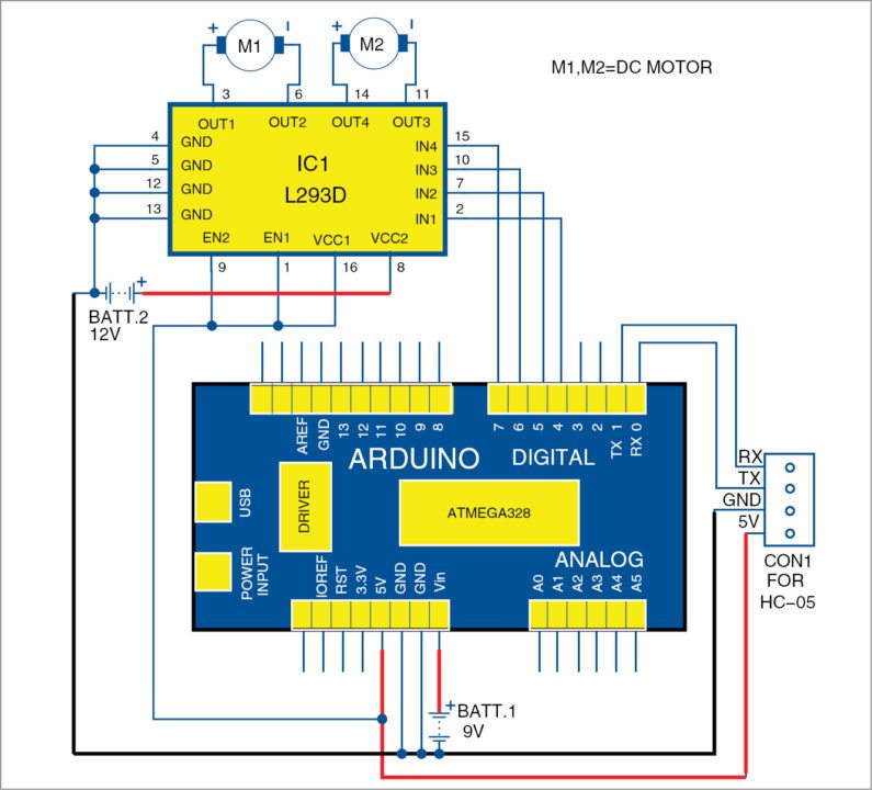
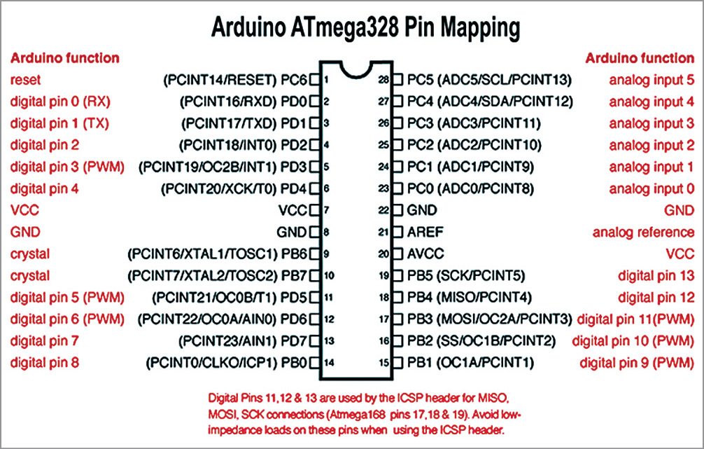
The circuit diagram of Arduino-based smartphone-controlled car is shown in Fig. 2. Pin mapping of the Arduino Uno is shown in Fig. 3.
Fig. 2: Circuit diagram of Arduino-based smartphone-controlled car
The ATmega328 chip on the Arduino Uno board comes with a bootloader, which allows you to burn the program to the chip without an external hardware programmer. After the chip is programmed, it can be removed from the board. The board can be powered from USB connection or external power supply such as batteries or AC/DC adaptors. After connecting the power supply to Vin pin, you get regulated 5V and 3.3V DC on the respective pins of the Arduino board. 5V is used to power the HC-05 Bluetooth module.
Fig. 3: Pin mapping of Arduino Uno
Serial pins 0 (RX) and 1 (TX) of Arduino are used to communicate with HC-05 module. Pins 4 through 7 are connected to H-bridge motor driver L293D IC. Out of these four pins, pins 5 and 6 provide 8-bit PWM output using analogWrite( ) function defined in the asc_car.ino Arduino sketch. Pins 2 and 3 of Arduino (not used in this project) can be used for additional functions like controlling lights, horn, etc.
Construction and testing
A 9V battery supply is used to power the Arduino Uno with its positive terminal connected to Vin pin and negative terminal connected to GND pin. 5V and GND (ground) pins from the Arduino are connected to HC-05 Bluetooth module. RX (pin 0) and TX (pin 1) pins of the Arduino are connected to TX and RX pins of the HC-05 module, respectively.
Pins 4 through 7 of the Arduino provide controlling signals for the motors. The Arduino outputs a very small voltage from these pins. So, an additional power supply is required to produce enough torque for the motors, for which H-Bridge L293D module is used. You can provide additional 12V power supply to pin 8 (VCC2) of L293D to drive the motors.
Output pins 4 through 7 of Arduino are connected to IN1 through IN4 pins of L293D, respectively. Ground pins 4, 5, 12 and 13 of L293D are connected to ground pins of the Arduino. The two 100 RPM geared DC motors (M1 and M2) are directly connected to output terminals of the L293D.
Mechanical arrangement of the bot or car is completed by attaching two wheels to the two motor shafts. Army directional wheels should be used on the front side of the car for moving towards left or right. (Castor wheel was used as the front wheel during testing at EFY Lab.)
The Arduino Uno can be programmed with the Arduino software (IDE). Switch off the Bluetooth module or disconnect it from Arduino while burning the asc_car.ino sketch into the Arduino Uno.
Connect smartphone with HC-05 module. After all the connections and mechanical arrangements are complete, download Arduino Bluetooth Controller app from Google Play Store in Android smartphone. There are many similar apps available on Play Store. This project uses ArduinoRC—an Arduino Bluetooth Controller app developed by Estacado’s Ltd.
Open the ArduinoRC application in Android smartphone and connect with the HC-05 device by typing ‘1234’ or ‘0000’ as pin for pairing with HC-05.
Feeding values in the app.
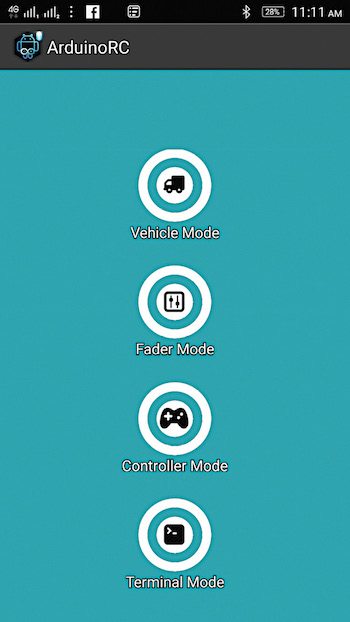
Press ‘Proceed’ option to connect your smartphone with the HC-05 module. You will see a screen on your Android phone as shown in Fig. 4. Select ‘Vehicle’ mode, open the menu in the top-right corner and select ‘Set Commands’ option. Set value ‘4’ for ‘Stop’ button in the application. Similarly, feed values 0, 1, 2 and 3 for Gesture_Front, Gesture_Left, Gesture_Right and Gesture_Back, respectively.
Fig. 4: Vehicle mode
Connect 12V battery supply to L293D module.
Now the bot is ready to be controlled with your smartphone. You can control your bot by tilting the smartphone in different positions. Tilt your phone forward or backward to move the bot in forward or backward direction. Similarly, tilt your phone to the right or left to make the bot take right or left turn, respectively.
With a slight tweak in the circuit, you can also use this app to control lights, horns and music systems by tilting the smartphone in different directions.
MeArm is an open-source hardware project, making the design freely available to anyone.
If you are building (or are considering building) your own MeArm you will find this video useful, especially as the MeArm assembly manual has a few errors that caused me grief that you’ll want to avoid.
Power versus performance is an ongoing battle, with the best involving a compromise between the two. High-performance system(s)-on-chip (SoC) designers often struggle to achieve the best possible performance-power balance. Customers’ user experience is an important aspect to consider as it determines performance improvements. However, this calls for increasing the battery size as most devices are battery-powered. Memory tracker technology from Performance-IP, for example, enables products to operate at higher efficiency, while reducing power consumption.
Power reduction techniques for processors
A typical SoC design consists of processors, memory clients, interconnects and memory systems. Processors are one of the major power consumers in a device, so switching off the CPU when idle helps. This includes turning off the processor when all processes are blocked, when processes appear to be busy waiting and extending real-time process sleep periods. Studies have shown these to increase battery lifetime by approximately 20 per cent in Apple systems.
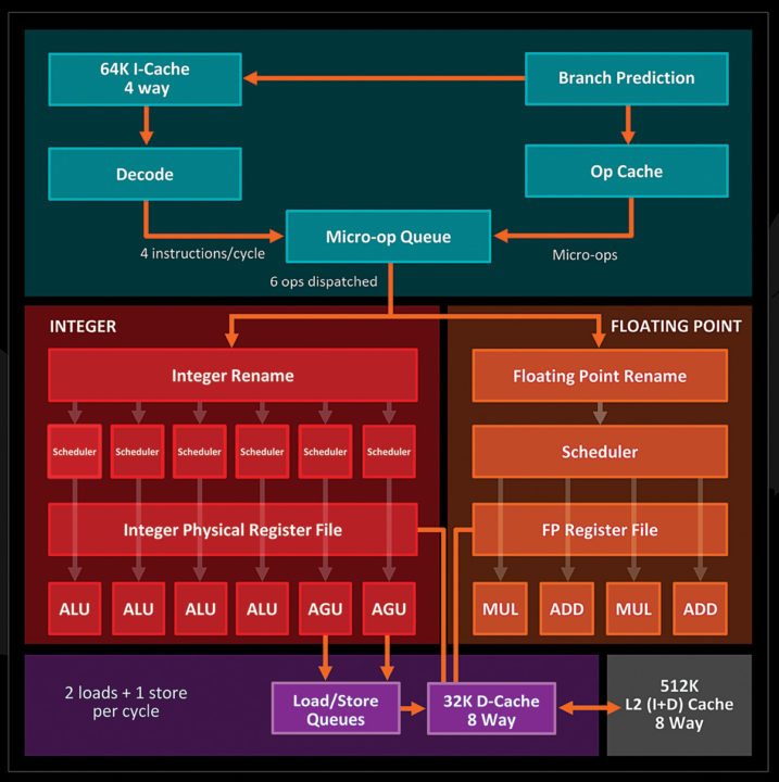
Fig. 1: Zen Core block diagram
These tricks are often used by processor designers as well. Dynamic power consumption in a processor arises from circuit activity. As performance, that is, speed and frequency, of the IC increases, the amount of dynamic power also increases. Dynamic power is data-dependent and closely tied to the number of transistors that change states. A hidden component of dynamic power is loss due to dynamic hazards. This must be taken care of while designing power-conscious processors.
Architectural changes to reduce power.
Crusoe from Transmeta is a very long instruction word (VLIW) processor designed for low-power applications including mobile PCs and Internet devices. It allows microprocessors to emulate Intel X86 instruction set. Instead of the instruction set being implemented on the hardware, Crusoe runs a software abstraction layer known as code morphing software.
This has brought about a reduction in required power. Intel processors at 400MHz used to consume about 7.4 watts, or AMD clocked at 700MHz at the time consumed 34 watts. The 700MHz Crusoe uses one watt, which was a revelation when introduced.
LongRun in Crusoe monitors the precise performance level needed by an application and dynamically adjusts the processor’s operating speed and voltage to match it. This increases the battery life by a significant amount.
Following this, there is SpeedStep from Intel that allows clock speed of the processor to be dynamically changed by the software. It allows the processor to meet the instantaneous performance needs of the operation being performed, thus minimising power consumption and loss through heat.
LongHaul is a speed-throttling technology developed by VIA Technologies that helps reduce power consumption. It uses specialised instructions utilised by the software to exercise control on bus-to-core frequency ratio and CPU core voltage. When the system boots up, ratio and voltage are set to hardware defaults. Depending on the load on the CPU, a CPU driver controls the throttling during operation.
Following a similar course, AMD’s dynamic frequency scaling and power saving known as PowerNow (mobile chips) and Cool‘n’Quiet (desktop and server chips) allowed adjusting clock speed under varying loads and idle conditions to save battery power. These power-saving techniques allowed power saving but, caused problems with the operating systems. Microsoft also reported problems previewing video files with SpeedStep enabled under Windows 2000 or XP. This called for making further changes, resulting in newer protocols that are being implemented today.
Power saving for the present.
Building up on PowerNow, AMD launched Turbo Core beginning with Bulldozer architecture. The architecture focused on reducing power consumption over the earlier K10 architecture for higher performance per watt.
Bulldozer processors are based on GlobalFoundries’ 32nm silicon on insulator, which reuses DEC approach for multitasking computer performance. By eliminating redundant elements that creep into multi-core designs, it aims to take advantage of its hardware capabilities while using less power.
This is followed by Zen architecture that looks to define balance between power and performance. As per multi-threaded Cinebench R15, performance per watt is more than double than it was for Piledriver architecture.
Zen architecture includes a complex stack engine that can eliminate certain stack manipulation instructions. This coupled with the core design, which is optimised to use less power, is something to look out for. It has an integrated power management controller that monitors and adjusts the voltage used by each core according to the temperature and loading.
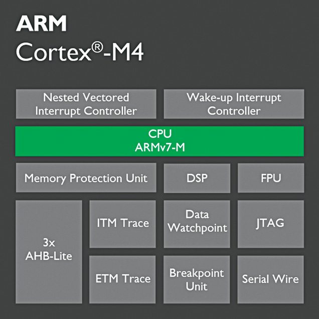
Fig. 2: Cortex M4 has been very popular with low-power processors for the IoT
Unlike previous versions, power management roles are baked directly into silicon and are out of the control of the software and operating system. The hardware on the chip can respond in a matter of milliseconds, allowing much tighter control over voltages and clock speeds.
Balancing power and performance.
Intel Turbo Boost draws a parallel with Turbo Core from AMD. However, Enhanced Intel SpeedStep Technology is more power conscious and allows the system to dynamically adjust processor voltage and core frequency, decreasing average power consumption and heat production.
Beijing, China – August 22, 2017 – Vicor Corporation (NASDAQ: VICR) today announced the introduction of Power-on-Package modular current multipliers for high performance, high current, CPU/GPU/ASIC (“XPU”) processors. By freeing up XPU socket pins and eliminating losses associated with delivery of current from the motherboard to the XPU, Vicor’s Power-on-Package solution enables higher current delivery for maximum XPU performance.
In response to the ever-increasing demands of high performance applications – artificial intelligence, machine learning, big data mining – XPU operating currents have risen to hundreds of Amperes. Point-of-Load power architectures in which high current power delivery units are placed close to the XPU, mitigate power distribution losses on the motherboard but do nothing to lessen interconnect challenges between the XPU and the motherboard. With increasing XPU currents, the remaining short distance to the XPU – the “last inch” – consisting of motherboard conductors and interconnects within the XPU socket has become a limiting factor in XPU performance and total system efficiency.
Vicor’s new Power-on-Package Modular Current Multipliers (“MCMs”) fit within the XPU package to expand upon the efficiency, density, and bandwidth advantages of Vicor’s Factorized Power Architecture, already established in 48V Direct-to-XPU motherboard applications by early adopters. As current multipliers, MCMs mounted on the XPU substrate under the XPU package lid, or outside of it, are driven at a fraction (e.g., 1/64th) of the XPU current from an external Modular Current Driver (MCD). The MCD, located on the motherboard, drives MCMs and accurately regulates the XPU voltage with high bandwidth and low noise. The solution profiled today, consisting of two MCMs and one MCD, enables delivery of up to 320A of continuous current to the XPU, with peak current capability of 640A.
With MCMs mounted directly to the XPU substrate, the XPU current delivered by the MCMs does not traverse the XPU socket. And, because the MCD drives MCMs at a low current, power from the MCD can be efficiently routed to MCMs reducing interconnect losses by 10X even though 90% of the XPU pins typically required for power delivery are reclaimed for expanded I/O functionality. Additional benefits include a simplified motherboard design and a substantial reduction in the minimum bypass capacitance required to keep the XPU within its voltage limits.
Two initial Power-on-Package devices are being introduced during the August 22nd Open Data Center Committee (ODCC) meeting in Beijing, China: a MCM3208S59Z01A6C00 Modular Current Multiplier (MCM) and a MCD3509S60E59D0C01 Modular Current Multiplier Driver (MCD). Multiple MCMs may be operated in parallel for increased current capability. The small (32mm x 8mm x 2.75mm) package and low noise characteristics of the MCM make it suitable for co-packaging with noise-sensitive, high performance ASICs, GPUs and CPUs. Operating temperature range is -40°C to +125°C. These devices represent the first in a portfolio of Power-on-Package solutions scalable to various XPU needs.
Over the past ten years Vicor has pioneered 48V Direct-to-XPU power development, reducing losses by an average of 25% every two years, while increasing power system density and cost-effectiveness. The MCM-MCD ChiP-set introduced today continues that evolution. By overcoming the obstacles imposed on XPUs by external high current delivery through the “last inch”, Vicor’s Power-on-Packagetechnology does more than just improve performance and simplify motherboard design – it enables XPUs to achieve previously unattainable performance levels that are necessary to fulfilling the promise of Artificial Intelligence.
When a human being starts learning in the early stages of life, every vision or simulation that takes place is recorded, compared and analysed almost instantaneously in the mind. It is complex, and we are gifted with a framework that helps us connect, recall and act to events.
In the machine world, intelligence must be taught to otherwise dumb machines. It is now possible to create a framework for them to think like us. Engineers have been working round the clock to perfect this, and as a result, software such as Caffe provide a gateway to deep learning.
Deep learning is a machine learning framework. To imbibe intelligent decision making into machines, deep learning smart algorithms must be devised. In short, it is the class of machine learning algorithm that forms a machine learning framework using which it obtains and processes real-life events.
Techniques include teaching and eventually creating a medium of interaction between man and machine. Machine vision and natural language processing are hot topics today, and any developer can play around with Caffe.
Fig. 1: Caffe installation
It is Caffe and it is brewed
Caffe is a deep learning framework. Its mantle circles around improving visual based image and video processing in optical devices such as cameras. Deep learning techniques can be combined with Caffe framework, and there are limitless possibilities that visual analytics provide. These could be your virtual eyes and brain, among others, for which the credit goes to advancements in sensor technology, high-performance graphic processing and evolving neural networks using advanced algorithms in this field.
How Caffe is brewed.
Data in the form of images and videos is what Caffe dines on. Data enters Caffe through data layers that lie at the bottom of nets. In some cases, it is sourced from databases (LevelDB or lightning memory mapped database) directly from memory or from files on the disk in HDF5 format, depending upon the use cases, and Caffe could be used to build models on it.
The models of Caffe work on deep networks that are made up of interconnected layers comprising chunks of data. Caffe has blobs or blob arrays that are used for storing, communicating and manipulating the information. It defines it in a net layer-by-layer model schema. The details of blob describe how information is stored and communicated in and across layers and nets because it is an N dimensional array.
The net follows the collection and connection of layers, which have two key responsibilities: constituting a forward pass for taking inputs and producing an output. The backward pass takes the gradient with respect to output, and computes the gradients with respect to parameters and to inputs, which are, in turn, back-propagated to earlier layers. All you need to do is define the setup, forward and backward passes for the layer, and it is ready for inclusion in a net.
Vision based use cases
Various uses cases of Caffe include surveillance and vision based alerting using Cloud and computer vision. Vision layers make room for the images from the real world as inputs and analyse colourations and spatial structures. These layers work by applying a particular operation to a region of the input and a corresponding region of the output, treating the spatial input as a vector with a specific dimension.
Getting down to the basics of video capturing, layers such as convolution get into action and are responsible for producing one feature map in the output image. Convolution is an important operation in signal and image processing, and in Caffe, pooling, cropping, edge detection and transformation processes take place in a sequence, followed by deconvolution and loss of learning.
Caffe learns about the real world
Software like Caffe learn about the real world by specifying a certain level of badness, driven by a factor called loss function. A loss function specifies the goal of learning by mapping parameter settings to a scalar value. Now, the goal of learning in machines is to find a setting of weights that minimise the loss function.
In Caffe, loss is computed by the forward pass of the network where each layer takes a set of input (bottom) blobs and produces a set of output (top) blobs. In simple words, the model works by comparing the loss while generating the gradient and then incorporating the gradient into a weight update that tries to minimise the loss. This is done by a solver in Caffe.
Fig. 2: Caffe deep learning framework
Significance of deep learning
Machines have made our lives easier and now we are one step closer to making these think. With deep learning, deep networks and tools like Caffe, it is now possible to make machines learn the way we humans have learnt in practical applications of speech recognition and image classification, among others.
What are the latest technology and industry trends that are shaping the world of power electronics? That’s what Rahul Chopra and Sneha Ambastha hoped to figure out by meeting Andy Gales, VP, Vicor—a global veteran of power electronics, who’s quite familiar with India and its engineering prowess, and has a passion for educating engineers on design of power electronics. Here are some excerpts…
Q. What are the broad trends shaping products that you see in power electronics?
Andy Gales, VP, Vicor
A. Miniaturisation is a major goal within the power electronics industry. Reducing size is always beneficial and even expected in electronics components.
Driving up the efficiency of both AC and DC systems, making systems more green, is also an important objectives for engineers. One of our big customers is in the data centre market where they don’t really care about the size but they do care a lot about the efficiency. If you are buying a megawatt of electricity even half a percent of efficiency is a big deal as it saves money on power bills and on air-conditioning as well.
Vicor has developed some innovative switching topologies like Sine Amplitude Conversion to help customers achieve their efficiency goals. Indeed, we spend a lot of time trying to improve the efficiency of all our products. For example one recently launched product, a bus converter module for high voltage DC applications, can provide a 48V, 24V or 12V output at up to 1.75kW from a 380V DC bus, at efficiencies of up to 98% in a package of just 61mm by 25mm by 7.2mm. All these products are manufactured in the USA.
“India Engineers are most interested in new technologies that enable them to quickly differentiate their solutions”
Q. Any new trends that you have seen in India?
A. Indian engineers are very knowledgeable about power. They are also very broad minded and they react quickly if they see an advantage in doing things a different way. It sometimes takes a bit longer in other countries to see adoption of new ideas. We enjoy working with Indian engineers, to help them optimise their solutions. I have been working in the Indian market for several years and find engineers interested in understanding the latest technologies available to help them design solutions more quickly.
Q. What are the technological advancements in Defence lately?
A. There is a big push in the Defence industry to reduce the size, weight and improve the performance of all types of systems. And this, of course, includes power supplies. Our latest DCM in a VIA package DC-DC Converter family, for example, increases the power density over our previous solutions by a factor of two. They also reduce weight by 50% and reduce waste heat by 45% due to efficiency gains. Performance is very important for a wide variety of defence applications. For example, if you are building a UAV, low weight is critical to maximize payload. Also, improved efficiency has a direct impact on how far and how long it can fly. The Defence market constantly struggles with size, weight, power and cost (SWaP-C) demands and Vicor’s component approach enables flexibility in optimizing for this criterion.
“There is a move in the Defence industry to reduce size, weight and to improve the performance of products.”
Q. What is the scope of your business in Defence electronics in India?
A. The business has been growing for many years. We started in India in the Defence market because our products are particularly attractive to engineers with challenging applications, where performance is Key. Today we are also talking to customers in the communications, industrial and automotive markets, also with demands for high performance.
Q. Are there any particular applications in Defence where your products may be useful?
A. Over the last 30 years our products have been used in a wide variety of Defense applications, from the traditional to the latest products enabled by the plethora of new technologies available. And what’s really exciting is that our products are helping companies to develop them. For example, one relatively new application is UAVs, where our new high power, low weight and small size products are critical to success. Yet the unique capabilities of our products are also enabling advances in other airborne applications like radar, and also in ground vehicle and naval applications. Here we are used in surveillance, monitoring, communications or in command and control systems, we power a broad array of Defence applications.
Q. How is India compared to China?
A. China is an important market for Vicor and there are some similarities. In terms of size probably India’s one tenth of China. But the Indian market is growing faster.
Q. Have you ever encountered the problem of counterfeit components in India?
A. Yes we have had some experience of counterfeiting. The safest thing to do is to buy the products from a reputable dealer.
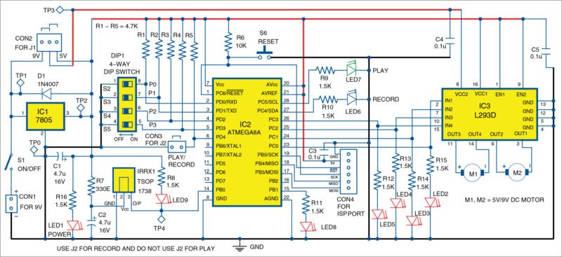
To control a robot, the signal is usually sent through a wireless system using radio frequency (RF) and infrared (IR). To send an IR signal, you need a transmitter and a receiver with an encoding and decoding system. The simple circuit presented here can control the movement of a robot using an IR remote that is used for a TV or DVD player, or an equivalent IR remote.
The basic working principle of this project is that the signal sent by the IR remote on pressing Play/Record button on the remote is saved in EEPROM of the microcontroller (MCU) in record mode. It plays back the same code (signal) when you press the same button in play mode. The program for the MCU can save 4-bit code (0 to F hex code) in record mode and output the same 4-bit code when the button is pressed in play mode.
Using the combination of these four bits, two motors installed on either side of the robot (third one being the caster wheel) can be controlled through a motor driver IC. Thus, different codes are used to control different movements of the robot.
Circuit and working
The circuit diagram of the remote-controlled robot is shown in Fig. 1. It is built around 5V voltage regulator 7805 (IC1), ATmega8A MCU (IC2), motor driver IC L293D (IC3), two DC motors (M1 and M2), IR receiver module TSOP1738 (IRRX1), 4-way DIP switch (DIP1), 5mm LEDs (LED1 through LED9) and a few other components.
Fig. 1: Circuit diagram of the remote-controlled robot
Once the circuit (or hardware) is ready, burn Remote_Robot.hex code to ATmega8A.
When power switch S1 is switched on, LED2 through LED7 glow for a while and turn off (self-test). Then, either LED6 or LED7 glows, indicating record or play mode, respectively. The mode depends on the setting of jumper J2.
In record mode, J2 is connected to the circuit and in play mode J2 is open. Press the required button on the remote once to record it. Then, permanently set J2 to play mode (that is, remove J2). If you want to change the code to other buttons, connect J2 to record mode.
For initial setup, either disconnect motors M1 and M2, or remove 5V/9V supply from J1 and then connect J2. Now, set the address code for the data (remote key) to be stored in the MCU using DIP switch DIP1 (using S2 through S5).
After setting the 4-bit address in hexadecimal code (say, 0101h), switch on the power using S1. After self-test, LED6 will glow, indicating the mode as recording. Press a button (say, 2) on the remote. LED9 will blink, indicating that a signal/data is received by IRRX1 sensor. This signal is fed to the MCU, which processes and saves data in its inbuilt EEPROM.
At the same time, a visual indication of the address being assigned for each data is indicated by the glowing of corresponding LED2 through LED5 in equivalent hexadecimal format.
Data being saved is acknowledged by the blinking of LED7. This process can be repeated for up to 16 required codes (0 to F hex).
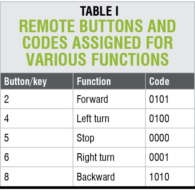
For easy control of the robot, we have assigned the code (or bits) to five buttons of the remote control as listed in Table I.
For any other button, the code is set as stop (0000). So to stop the robot in an emergency case, press any other button on the remote.
After recording the required codes, remove J2 and press reset switch S6. After self-test, LED7 will glow, indicating that it is in play mode. Now, press the programmed remote button randomly and check that LED2 through LED5 indicate the required code. LED8 will blink for a while if there are errors like a button not pressed properly or signal not received properly.
Software
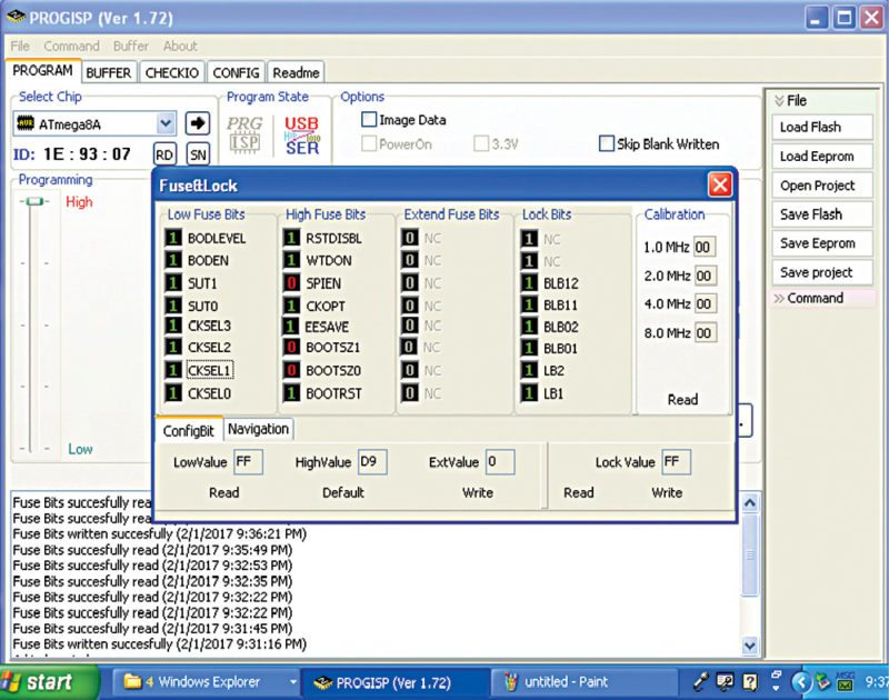
The software (remote_robot.c) is written in C language and compiled using Atmel Studio. AVR PROGISP programmer is used for programming the MCU during testing. However, you can use any suitable programmer for the same.
Burn remote_robot.hex file to the MCU through ISP port. Since the MCU uses an internal oscillator, set the fuse bits to the default value as shown in Fig. 2.
Fig. 2: Screenshot of fuse bit settings
Note. As per datasheet of ATmega8A, fuse setting 1 means unprogrammed and 0 means programmed.
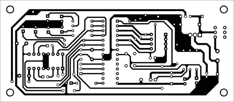
An actual-size, single-side PCB layout for the remote-controlled robot is shown in Fig. 3 and its components layout in Fig. 4. After assembling the circuit, place the populated PCB and 9V battery on the chasis of the robot. J1 is used to select 5V or 9V power supply depending on 5V DC motors or 9V DC motors used.
Fig. 3: PCB layout of the remote-controlled robotFig. 4: Components layout of the PCB
Download PCB and component layout PDFs: click here
Use of an IC base/socket is recommended for the MCU. Connect M1 and M2 to the PCB through twin-wire external wires. Before running the robot, verify the voltages are as shown in Table II. Your remote-controlled robot is ready to use!
3W rated 2817 size metal foil on ceramic chip resistors support 1A to 30A applications
Woking, UK, 21 August 2017 – TT Electronics, today extended its MFC series of metal foil chip resistors with a new 2817 size that can dissipate up to 3W. Ideal for current sensing in the 1A to 30A range, the MFC2817 chip resistors enable designers to achieve highly compact power conversion circuits in demanding industrial and medical applications.
In addition to power supply and DC-DC converters, these metal foil on ceramic resistors, also meet the current measurement requirements of driver circuits for motors, actuators, lighting and HVAC systems. This growing market for distributed power management and motion control faces pressure to reduce power loss whilst maintaining accuracy, leading to a demand for lower ohmic values and reduced TCRs. The MFC2817 addresses this need with values from 3m to 150m and a low TCR of 30ppm/°C compared to the 4m minimum value and 50 – 100ppm TCR specification of the nearest competitive part.
Metal foil on ceramic technology provides superior reliability compared to other resistor technologies: its surge tolerance is better than thick-film resistors ensuring improved reliability in the presence of current surges; and its self-heating is lower than thick-film or metal-strip types, which avoids hot-spots and further improves product reliability.
Safely absorb repetitive ESD strikes without performance degradation
Beijing, China, August 22, 2017 —Littelfuse, Inc., the global leader in circuit protection, today introduced 80A discrete bidirectional TVS Diode Arrays as the latest addition to its SP11xx Series TVS Diode Arrays (SPA® Diodes). SP1103C Series 80A Discrete Bidirectional TVS Diodes offer circuit designers lower standoff voltage options for protecting lower voltage power buses from electrostatic discharge (ESD) damage.
SP1103C Series TVS Diode Arrays
Constructed using TVS diodes fabricated in a proprietary silicon avalanche technology, these diodes protect each I/O pin to provide a high level of protection for electronic equipment sensitive to destructive ESDs. These robust diodes can safely absorb repetitive ESD strikes at ±30kV without performance degradation. Additionally, each diode can safely dissipate 80A of 8/20µs surge current with very low clamping voltages.
Applications for SP1103C Series TVS Diode Arrays are commonly found in automotive electronics, industrial products, consumer electronics, switches/buttons, test equipment/instrumentation, point-of-sale terminals, medical equipment, notebooks/desktops/servers and computer peripherals.
“The enhanced ESD capability the SP1103C Series enables manufacturers to achieve ESD protection beyond the maximum level stated in the IEC standard,” said Tim Micun, business development manager for TVS Diode Arrays at Littelfuse. “It also protects against a multitude of other threats to ensure greater product reliability in the field.”
SP1103C Series TVS Diode Arrays offer these key benefits:
• Extremely low (0.01 ohm) dynamic resistance ensures fast-acting ESD protection during an overvoltage event.
• Discrete bidirectional design allows them to work whether they are inserted forward or backward.
• Low breakdown voltages (3.3V) protect power rails up to 2.8V.
• Industry-standard leadless 1610DFN package is suitable for use in industrial, automotive, and commercial environments.
New Delhi, August 24th 2017 — Analog Devices, Inc. announced today a collaboration with The Cornucopia Project and ripe.io to explore the local food supply chain and use this work as a vehicle for educating students at ConVal Regional High School in Peterborough, N.H., and local farmers on 21st century agriculture skills. The initiative instructs student farmers how to use Internet of Things and blockchain technologies to track the conditions and movement of produce from “Farm to Fork” to make decisions that improve quality, yields, and profitability. Together with the Cornucopia Project, the endeavor is funded by Analog Devices and ripe.io, with both companies also providing technical training.
For the project, Analog Devices is providing a prototype version of its crop monitoring solution, which will be capable of measuring environmental factors that help farmers make sound decisions about crops related to irrigation, fertilization, pest management, and harvesting. The sensor-to-cloud, Internet of Things solution enables farmers to make better decisions based on accumulated learning from the near-real-time monitoring. These 24/7 measurements are combined with a near infrared (NIR) miniaturized spectrometer that conducts non-destructive analysis of food quality not previously possible in a farm environment.
“This project expands on our ‘Internet of Tomatoes’ program which empowers farmers to make better decisions throughout the growing cycle, improving quality, economic, and environmental outcomes,” said Kevin Carlin, vice president, Automation, Energy and Sensors, Analog Devices. “Our crop monitoring solution will provide reliable and precise information to student farmers and local farmers so they can grow healthier, fresher, better tasting produce. It demonstrates how a crop monitoring solution extends the value and possibilities of the Internet of Things in truly transformative ways.”
The Cornucopia Project, a non-profit located in Peterborough, N.H., provides garden and agricultural programs to students from elementary through high school. Student farmers in its Farm to Fork program learn how to use advanced sensor instrumentation in their greenhouse, which provide valuable data to assess the attributes of tomatoes, and how these factors affect taste and quality. The program also educates students on how crops can be tracked throughout the agricultural supply chain to support food quality, sustainability, traceability, and nutrition.
“Analog Devices is helping us explore how advances in technology can support local food systems,” said Karen Hatcher, executive director, The Cornucopia Project. “We are training next-generation farmers in 21st century agriculture to harvest tastier, more abundant and more sustainably grown tomatoes than ever before. This initiative will contribute to enhancing the economic health and vitality of local small- and medium-size farms and the communities that support them.”
ripe.io is contributing its blockchain technology to model the entire fresh produce supply chain, combining the crop growing data, transportation, and storage conditions. Blockchain – a distributed ledger, consensus data technology that is used to maintain a continuously growing list of records – will track crop lifecycle from seed to distributor to retailer to consumer, bringing transparency and accountability to the agricultural supply chain.
“This project is one of the first implementations of blockchain technology to build an open and transparent supply chain with farmers, suppliers, distributors, retailers, food service, and end consumers,” said Raja Ramachandran, CEO of ripe.io. “What is learned in the initiative not only will improve quality, economic, and environmental outcomes in the local farming community, but also can be extended to other farms and crop species around the country.”
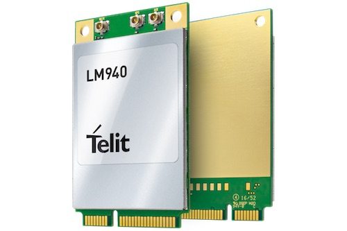
Telit’s new industrial-grade LM940 Mini Card is the first in its class embedded with Qualcomm® Snapdragon X12 LTE Modem supporting download speeds of up to 600 Mbps
As the fastest LTE-Advanced Mini Card, the LM940 is available for immediate deployment
New Delhi, August 21, 2017 – Telit, a global enabler of the Internet of Things (IoT), today announced the LM940, the world’s first global Full PCI Express Mini Card (mPCIe) module for the router and gateway industry supporting LTE Advanced Category 11 (Cat 11) with speeds of up to 600 Mbps, available with various mobile network operator approvals in the fourth quarter of 2017.
The only enabling technology in an mPCIe form factor to support Cat 11 with the Snapdragon X12 LTE modem, the industrial-grade LM940 delivers significant flexibility and a competitive edge to original equipment manufacturers (OEM) looking to quickly deploy next generation products with an unrivaled user experience.
Today, customers of router and gateway OEMs demand additional bandwidth and near instant network response times as applications like high definition video streaming with digital signage, commercial and enterprise failover needs and pop-up stores are becoming increasingly sophisticated.
“This industrial-grade module from Telit supporting LTE Cat 11 with global coverage will be very attractive for equipment manufacturers looking to deploy the latest solutions now, especially in the router and gateway marketsupporting high-bandwidth dependent applications like digital signage,” said Sam Lucero, senior principal analyst for IHS Markit, a global information provider. “As detailed in our June 2016 report on the industrial cellular IoT gateways market*, IHS Markit anticipates gateway shipments will rise from nearly two million shipped in 2016 to more than six million shipped in 2021. The value of these industrial cellular IoT gateways shipped in 2021 will slightly exceed USD $1.6 billion.“
“Telit extends its leadership again by delivering customers the latest releases in LTE Advanced technology that they can take to market today,” says Manish Watwani, VP Global Product Marketing for Telit. “The LM940 is the only global product for the router and gateway segment that allows OEMs to immediately leverage the 3x carrier aggregation and the higher order modulation of the 256 QAM capabilities currently available amongst most mobile operator networks. Combined with an exceptional power efficiency platform, this is by far the ideal solution to enable commercial and enterprise applications in the router industry, such as branch office connectivity, LTE failover, digital signage, kiosks, pop-up stores, vehicle routers, construction sites and more.”
“The Snapdragon X12 LTE modem with LTE Advanced technologies providing peak download speeds of 600 Mbps, defines a new level of service for emerging applications,” says Gautam Sheoran, director, product management, Qualcomm Technologies, Inc. “We are pleased with our ongoing collaboration with Telit to bring technologies that enable emerging applications like 4K video, virtual reality and cognitive computing to the global market.“
Additional Technical Features:
LTE Category 11 LTE Cat. 11 DL / Cat. 5 UL Rel.10
3x Carrier Aggregation leverages extended capabilities of the network for increased coverage and bandwidth
Up to 600 Mbps DL w/3x Carrier Aggregation and 256 QAM
Up to 75 Mbps UL w/ 64QAM
Car companies have developed a design for universal data format that will allow for standardised vehicle data exchange, making the crowd sourcing paradigm available for self-driving automobiles. Sharing data such as real-time traffic, weather and parking spaces will be much faster and easier. The design is called sensor ingestion interface specification (SENSORIS), and it has been picked up by ERTICO – ITS Europe. It is a UK body overseeing the development of globally-adopted standards related to future automotive and transportation technologies.
The aim is to define a standardised interface for exchanging information between in-vehicle sensors and a dedicated Cloud as well as between Clouds that will enable broad access, delivery and processing of vehicle sensor data, enable easy exchange of vehicle sensor data between all players and enable enriched location based services that are key for mobility services as well as for automated driving.
Currently, 11 major automotive and supplier companies have signed up for SENSORIS innovation platform. These are AISIN AW, Robert Bosch, Continental, Daimler, Elektrobit, HARMAN, HERE, LG Electronics, NavInfo, PIONEER and TomTom. Pooling analogous vehicle data from millions of vehicles around the world will allow for a fully-automated driving experience. Each vehicle will have access to near-real-time info of road conditions, traffic data and various hazards that will help these self-driving vehicles make better decisions on the road.
Many of today’s futuristic projects—from self-driving cars to advanced robots to the Internet of Things (IoT) applications for smart cities, smart homes and smart health—rely on data from sensors of various kinds. To achieve machine learning and other complex technical goals, enormous quantities of data must be gathered, synthesised, analysed and turned into action, in real time.
A self-driving car uses complex image recognition and a radar/lidar system to detect objects on the road. The objects could be fixed (curbs, traffic signals, lane markings) or moving (other vehicles, bicycles, pedestrians). The scope involves validating the data of more than 1000 hours of car camera and radar/lidar recordings. At three frames per second, there are almost 11 million images to analyse and correct, which is too many to do using off-the-shelf tools.
Architecture for a tool enabling the car system is meant to validate large amounts of information provided by real, direct observations—also known as ground-truth data. Creation of the tool provides a way to validate the accuracy of sensor-derived data, and to make sure that the car would respond appropriately to actual objects and events, and not to sensor artefacts.
The future self-driving vehicle value chain will be driven by software feature sets, low system costs plus high-performance hardware. Simulation software based on agent based modelling methodology, which is used to create real-world driving scenarios to test complex driving situations for autonomous vehicles in agent based simulation in terms of advancing virtual testing and validation, will be used to test future autonomous vehicle concepts. This method of testing puts agents (vehicles, people, infrastructure) with specific driving characteristics (such as selfish, aggressive, defensive) with their connections in a defined environment (cities, test tracks, military installations) to understand complex interactions that occur during simulation testing.
Benefits to car manufacturers and their suppliers that this approach aims to deliver are faster product development cycles, reduced costs related to test vehicle damage and lower risk of harming a vehicle occupant under test conditions.
The goal has always been to find a home for this specification that is open, global and accessible to all. This is a vital step on the path to creating a shared information network for safer roads. If a car around the next corner hits the brakes because there is an obstruction, that information could be used to signal to the drivers behind to slow down ahead of time, resulting in smoother, more efficient journeys and lower risk of accidents. But that can only work if all cars can speak and understand the same language.
SENSORIS
Vehicles driving on the road are equipped with a magnitude of sensors. This sensor data may be transferred over any kind of technology from the vehicle to an analytic processing backend. Between individual vehicles and the analytic processing backend, an OEM or system vendor backend may be located as a proxy.
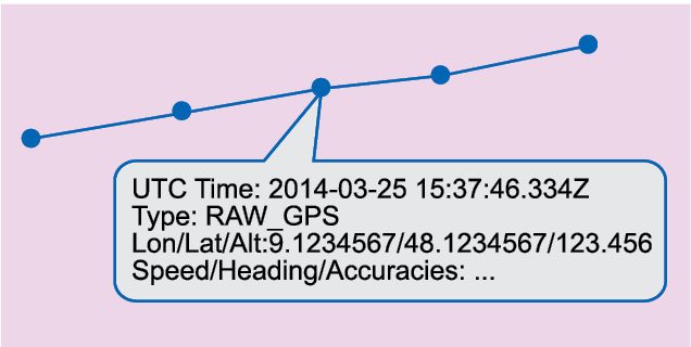
The sensor data interface specification defines the content of sensor data messages and their encoding format(s) as these are submitted to the analytic processing backend. However, the specification may be used between other components as well. Sensor data is submitted as messages with various types of content. It is common to all kinds of submitted messages as these are related to one or multiple locations.
Fig. 1: Paths
Sensor data messages may be time-critical and submitted near-real-time but also may be of informational value and submitted with an acceptable delay accumulated within other data. Neither priority nor requirements on latency are part of the specification. The content and format of sensor data messages is independent of submission latency (in near-real-time or delayed).
When it comes to low-power portable devices, why not rely on a single battery for the power? I see many such applications that require two or three primary batteries, which seems pretty wasteful. After all, by using a readily available, low-cost switching regulator chip, you can power your portable device with a single battery.
Multiple batteries, of course, increase the voltage. But you can achieve the same with a great, high-efficiency boost converter. What’s more, the converter will also maintain a nice regulated supply for the device. With the advantages in efficiency and small size, this really is a sweet application idea.
Suppose you need a 3.3V supply and want to extract as much energy as possible out of your battery. You could use a non-rechargeable, standard-type primary AAA or AA size battery. Comprised of alkaline or lithium, these batteries offer much higher energy density than any rechargeable cell.
Alkaline batteries cost about one-third that of lithium. However, since alkaline batteries have a higher internal resistance, they function better at low discharge rates. Also, at about 210Wh/kg, they have about one-half the energy density of 1.5V lithium primary cells (Li-FeS2). Under a high load, an alkaline cell’s output voltage will sag due to the high internal Z. A spent alkaline in a digital camera (a high peak load) will leave enough energy to run the kitchen clock for two years. The Energizer Ultimate Lithium brand is an example of a lithium Li-FeS2 type battery (1.5V), providing a 400WH/kg energy density and relatively low impedance.
A Closer Look at 3.6V Primary Lithium-Ion Batteries
Lithium-thionyl chloride (LiSOCI2 or LTC) is another kind of lithium battery that I’d like to highlight. While LiSOCI2 is not generally found in the drug store and is quite a bit more expensive than the Li-FeS2 type, it does provide an energy density of up to 500WH/kg. With a nominal voltage of 3.60V/cell, it is also one of the most rugged of the lithium-metal batteries. LiSOCI2 cells offer an even higher energy density than the 1.5V Li-FeS2 type.
I also must mention that the LiSOCI2 3.6V batteries are available in bobbin and spirally wound versions. The bobbin-type have higher internal impedance, but provide a higher energy density and a very low self-discharge rate (<1%/yr). As a result, the bobbin-type can operate up to 40 years in a very low-current application.
The use of 3.6V lithium-ion batteries has become common. However, because the battery voltage ranges between 2.7V and 4.2V, a step-up/step-down DC-DC converter is needed to make a standard 3.3V supply.
While there are various topologies that can be used for a combination step-up/step-down converter, the most popular is the single-ended primary inductance converter (SEPIC). This is a non-isolating voltage converter that is unusually non-inverting, though it can also be inverting.
Another method that many don’t consider is using a step-up converter followed by a low dropout (LDO) regulator. Because a linear regulator is used for the step-down function, many assume that it has poor efficiency. However, when making 3.3V from a single lithium-ion battery, the efficiency of this circuit can exceed that of an equivalent SEPIC circuit.
There are also the added advantages of lower component count, lower cost, and less board space.
Boost Regulators with Ultra-Low Quiescent Current
As an example of a boost regulator that can support single-battery portable devices, let’s consider the MAX17220–MAX17225 family of boost (step-up) DC-DC converter ICs from Maxim. Figure 1 provides a circuit drawing. These ICs offer 225mA, 0.5A, or 1A peak inductor current and feature a 0.40V minimum VIN. They have ultra-low quiescent current and a True Shutdown mode that disconnects the output from the input without forward or reverse current. Their output voltage is selectable with a standard 1% resistor. Since the converters have a built-in power switch, the circuit design requires only four external components.
Fig. 1: MAX17220–MAX17225 Basic Circuit
The MAX17220-MAX17225 converters are suited for small, battery-powered portable designs because they come in a very small total solution size and provide high efficiency (up to 95%) throughout their entire load range (see Figure 2 for a block diagram). Their switching frequency is up to 2.5MHz, and their low quiescent current helps extend battery life. For easy PCB layout, they are available in 2 x 2mm 6-pin μDFN or 0.88 x 1.4mm 6-bump WLP packages.
Any battery, may it be a lead acid or a Li-ion battery, has to be tested multiple times to test the battery capacity, leakage resistance and the time battery capacity can withstand. For these types of processes, a human cannot sit in front of the setup to record the voltage, current, cycle count and other values. To simplify this job a LabVIEW Graphical User Interface (GUI) can be made to automate the whole process.
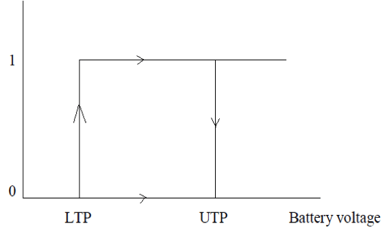
Every battery which has to be charged or discharged, has two significant limits, Lower Threshold Point (LTP) and the Upper Threshold Point (UTP). When the battery starts charging and reaches UTP, a relay is automatically switched on and starts discharging. Two relays with a provision of sensing voltage and current are included for this charging and discharging cycle.
Cyclic charging and discharging cycle
A cyclic process has to involved while programming in LabVIEW, which resembles an SR flip flop as shown in Figure 1 below;
Fig: Cyclic Process for a battery
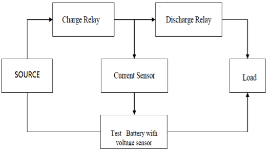
Here the source may be a constant current source or constant voltage source. Used here are the NI-9222 card, which is an Analog input/output sensor, NI-9148, which is an Relay module and a chassis for connecting all these modules to a PC through Ethernet which is an NI-9188, a cDAQ (compact Data Acquisition). The block diagram for the process is shown below;
Fig: Block Diagram of the process which has been automated
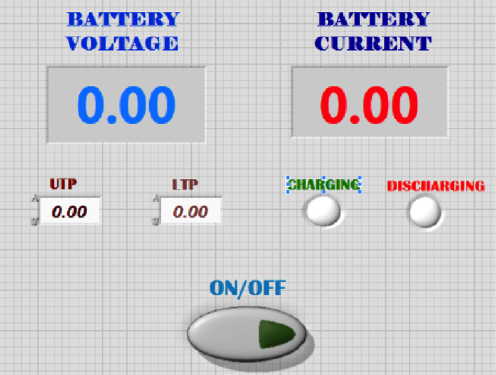
LabVIEW Panel
LabVIEW is a user-friendly software for graphical coding. It has a front panel for user interface and block diagram where the entire code is developed. The basic GUI has a provision to set UTP and LTP points, voltage and current of the battery, whether it is charging or discharging. This is designed basically to see the battery leakage resistance or measure the time in which it is going into discharging mode. A manual switch is given by pressing it only when the system starts.
Fig: Basic GUI for testing the battery
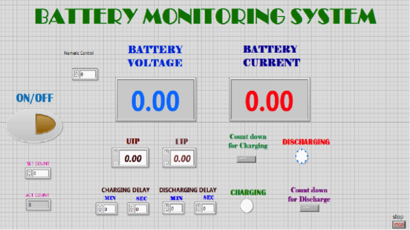
The final GUI is made with all provisions to give number of counts or cycles, delay in charging and discharging cycles, indications for which phase of the cycle it is in. The below figure shows the outline of the user interface panel, where all the above indications can be seen. Provision for displaying actual count and the set count is also available.
Once all the connections with the source, including the modules and the battery are made, then only the application panel with all values is executed. You might forgot to set any value or if you set any reverse values it has to be indicated, otherwise the battery may be destroyed.
Fig: Final GUI with all displays involved
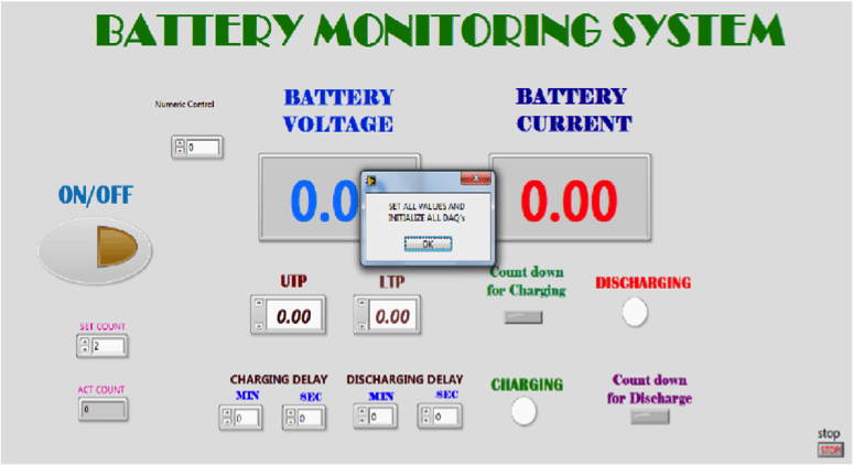
Those popup should arrive as soon as the application is executed. Below is an example to set the initial values. By initializing all values, the VI executes and a manual ON/OFF button is provided to start the process or stop whenever needed between the cycles.
Fig: Pop-up display if by mistake the VI is run without values
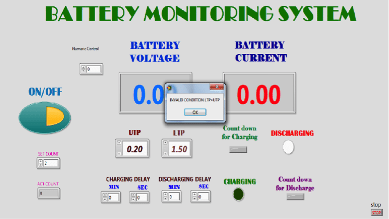
Without differentiating the UTP and LTP, as LTP should be less than UTP an error might popup. Any error while adjusting these values also shows a popup to indicate an invalid condition as shown below;
Fig: Pop-up if the values given reversed
If all the conditions are satisfied then the process can be executed any number of times. There is a provision for the data to be recorded in the database with all voltage, current, time for charging and discharging. For turning it on and off, a manual switch and an emergency stop button is also provided. The internal block diagram has a provision to save the database in an excel sheet of all values.
The human mind is arguably the most complex in this world. Utterly fascinating, it is an object of admiration to everyone. Some people take this admiration to a higher level and try to understand how the brain does what it does. Others go even further and attempt to replicate this marvel of a creation. While this is no mean task, science is a lot closer to creating artificial intelligence (AI) today than it was a few years ago.
This article takes you through a tool that provides an environment for R&D in AI domain. Be it to make a software application smarter or to create your own clone, this tool provides the very basic raw materials you need to start with, and may be carves out a path and guides you along. But, it is no cake-walk. The tool we are talking about is OpenCog.
Apt for research in AI
OpenCog is an open source software project, which aims to create an open source framework for artificial general intelligence. The developers state, “We are undertaking serious effort to build a thinking machine.” While this is stretching it too far for the present, the team behind OpenCog presently aims at nurturing the R&D environment and creating a code that can help make smarter systems, and working towards developing cognitive capability at the human level.
OpenCog has been developed by OpenCog Foundation under GNU Affero general-public licence and is supported by Artificial General Intelligence Research Institute (AGIRI), Google Summer of Code project and others. It is written using a combination of C++, Python and Scheme, and is built for Linux platform. The software is currently under an early stage of development, and is mostly useful for building applications that require significant AI capability. This is an interesting and powerful AI platform, but you will need to make significant customisations and integrations to get your projects up and running.
Fig. 1: MicroPsi architecture, an implementation of OpenPsi
Keeping the first foot forward
Prime inspiration for the project is the artificial general intelligence theories by Dr Ben Goertze. The concept of probabilistic logic networks is made extensive use of, to robustly handle uncertainty and perform effective reasoning in real-world circumstances. The idea is a novel conceptual, mathematical and computational approach to uncertain inference.
Well, you have seen what to expect from this tool, but it is still not clear as to how you can go about working with it. Building a cognitive system is easier said than done, and certainly that much more complicated for someone just beginning to work with AI. Let us begin by trying to understand how OpenCog goes about creating AI.
The knowledge base.
The first step is to create a system that stands for the knowledge inside the memory of an intelligent system, called knowledge representation. While this details the basic nature and organisation of knowledge components, it could be highly complex and dynamic, or simple, static and easy to describe. The catch here is how explanatory you want the knowledge representation to be. Does it have to be a repeated looping of a basic element, specialising for different situations? Or, does it have to be based on a learning algorithm that develops knowledge representations as time progresses? In OpenCog, they call this knowledge representation AtomSpace.
AtomSpace, the very basic.
It is in AtomSpace that different components of the intelligent system you have in mind are held, and this is also the query/reasoning engine that fetches data, manipulates it and performs reasoning on it. Effectively, AtomSpace is a kind of graph database, where graphs are representations of data and procedures. What this means is that graphs can be data, executable programs or data structures. AtomSpace could also have hypergraphs. The vertices and edges of the graphs are atoms, which essentially capture the notion of an atomic formula in mathematical logic.
How to use these to develop your system
What you have to do is use atoms to form small portions of the mind, which when put together form the complete system. You cannot code line-by-line per se, as the system is built for use by automation and machine learning engines. Automated sub-systems manipulate, query and inference over data or programs, and work to manipulate networks of probabilistic data by means of rules, inferences and reasoning systems. These are similar to an extension of probabilistic logic networks to a generalised system where data is automatically managed.
Atomese, the programming language.
The above programming-like language is informally referred to as Atomese. Developers describe Atomese as a strange mash-up of SQL, prolog/datalog, lisp/scheme, haskell/caml and rule engines. Most engines provide basic atoms that represent relations like similarity, inheritance; logic like Boolean or, there-exists; for Bayesian and other probabilistic relations; intuitionist logic like absence and choice; thread execution; and expressions including variables, mapping or constraints. As a programming language, Atomese is probably inefficient, slow and not scalable, but powerful as an input to automation sub-systems.
In this video, the presenter is going to construct a system using Arduino Nano, LED Strips, 12 V power supply which will be able to control the intensity of the LEDs.
The intensity of the LEDs is controlled by scrolling the computer mouse.
Electromagnetic interference (EMI), also called radio-frequency interference (RFI) when in the radio frequency spectrum, is a disturbance generated by an external source that affects an electrical circuit by electromagnetic induction, electrostatic coupling, or conduction.
Electromagnetic compatibility (EMC) is the ability of electrical or electronic equipment/systems to function in the intended operating environment without causing or experiencing performance degradation due to intentional EMI.
Upon completion of the slideshow, you will be able to understand:
EM Signals
Various related definitions
Basic Elements of EMI
Classification of EMI
Radiated Interference
Conducted Interference
Difference between Intra system EMI and Inter System EMI
A solar panel is made up of solar cells that convert solar energy (sunlight) to electricity. This conversion is known as photovoltaic effect. Solar energy is the best alternate energy source as it is renewable, easy to produce and saves the environment. The government of India too promotes it by providing remarkable subsidies.
Basic structure of a solar cell and its working principle
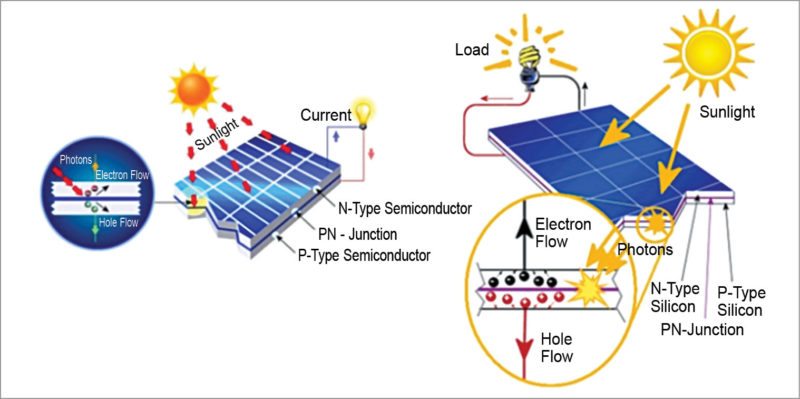
A solar cell, also known as a photovoltaic cell, works on the principle of photoelectric effect—ability of an object to emit electrons when light falls on it. To generate electricity from a solar cell, a material is required that emits electrons and is raised to a higher energy state by the absorption of light. These electrons have enough energy to drive the connected device or load. The cells are made of a semiconductor material that is used in the form of p-n junctions.
A solar cell consists of n-type (having electrons as a majority charge carrier) and p-type (having holes as a majority charge carrier) semiconductor materials. The depletion region is formed between n-type and p-type materials. The depletion layer is made up of positive and negative ions. Electrons and holes are not present inside the depletion layer. Light travels in the form of packets of energy called photons. These photons (sunlight) are applied on the depletion region.
Photons are absorbed in depletion regions and generate electron-hole pairs. These free electrons and holes have enough energy to jump out of the depletion zone. If a wire is connected from the cathode (n-type material) to the anode (p-type material), electrons flow through the wire. The electrons have negative charge and, hence, get attracted by p-type material (positive terminal), travel through the external load (device) and create a flow of electrons (current), as shown in Fig. 1.
Fig. 1: Working principle of a solar cell
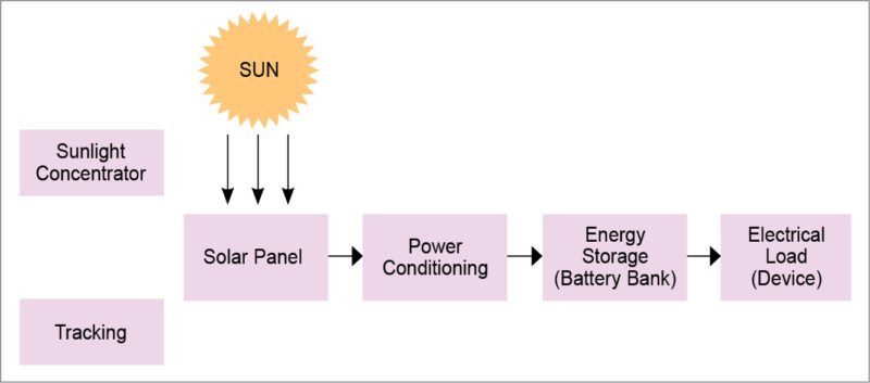
As shown in Fig. 2, the sunlight concentrator focuses sunlight on a small part and tracks the Sun throughout the day for higher efficiency. The solar panel generates unstable or fluctuating electricity and, thus, has to be regulated. The power-conditioning block gives regulated stable electricity that is stored in the battery or a battery bank. The battery gets damaged if a proper power-conditioning circuit is not used. The device gets energy from the battery.
Sometimes, a solid copper foundation is laid over the solar panel that gives it massive strength. Solar panels may have anti-reflective (AR) coating over the surface to produce more energy and increase efficiency. AR layer usually has NaOH surface texturation with several tiny pyramids. The layer’s thickness should be designed for better efficiency.
Fig. 2: Block diagram of a solar system
Multi-junction structure of a solar cell
A few years ago, late Dr A.P.J. Abdul Kalam said that, we are not utilising solar energy efficiently. Researchers are working hard and have come up with different solar structures and technologies to increase the efficiency of solar cells. Till now, we have depended on single-junction solar cells that give an efficiency of about 20 per cent. To improve this efficiency, the concept of multi-junction solar cells has been adopted. These are solar cells with multiple p-n junctions made up of different semiconductor materials.
The gap between valance band and conduction band is called forbidden gap or energy gap (Eg). In an energy band diagram, electrons jump from valence to conduction band and become free when electrons absorb enough energy. These electrons are considered free electrons and take part in current flow. If an applied photon has wavelength greater than or equal to hc/Eg (h is Plank’s constant and c is velocity of light), electrons gain enough energy and jump from valence to conduction band.
Electrons that belong to conduction band take part in current flow and are thus responsible for generating electricity. In the above-mentioned relationship, h and c are constant, which means the number of free electrons depends on Eg. This Physics fundamental has been used in the structure of solar cells. A multi-junction structure (material with different values of Eg) absorbs maximum sunlight (broad range of wavelengths), generates more free electrons or current and, ultimately, increases the efficiency of solar cells.
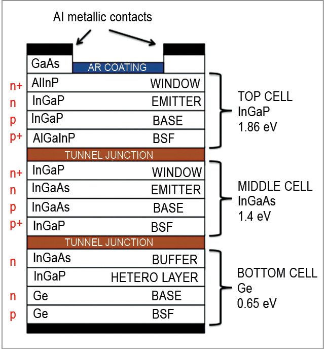
The top-most junction has the widest band gap and, as we go down, it decreases. It is necessary to find the best semiconductor materials in terms of band gap to increase efficiency. Fig. 3 shows the different semiconductor materials used in a multi-junction solar cell. As photons (sunlight) strike the solar cell, highest energy-level photons are absorbed by the top-most layer, and photons with low energy are absorbed in the lower layers.
Fig. 3: Structure of a multi-junction solar cell
A window layer is used to reduce surface recombination velocity, and the back surface field (BSF) layer reduces the scattering of carriers towards the tunnel junction. It simply functions as an electrical contact and, thus, covers the entire back surface of the cell structure. It is always made of metal.
 The much-beloved Internet of Things has come to fundamentally reshape how firms in virtually every industry operate. Nonetheless, the 21st century phenomenon that’s connected us all has some significant downsides, chief among them its vulnerability to outside attacks.
 The Internet of Things is comprised of a wildly diverse range of device types- from small to large, from simple to complex – from consumer gadgets to sophisticated systems found in DoD, utility and industrial/manufacturing systems.
 The HBO hack is just one recent example of how cyberattackers are now targeting corporations, and CyberArk chief Udi Mokady said that bitcoin is often used to pay them off. “That’s the requirement of most of these hackers,” the founder, chairman and CEO told “Mad Money” host Jim Cramer on Tuesday. “Many companies choose to buy bitcoin in some state or fashion and pay them off. “Bitcoin, an increasingly popular cryptocurrency, has surged in price in 2017, having climbed nearly 300 percent year to date.
 Nowadays smartphones can be used to control a host of electrical and electronic devices including motors, music systems and lights. Here we present an Arduino based robot car, which can be controlled using an Android smartphone having ArduinoRC application installed in it. This bot receives commands from your smartphone with the help of a Bluetooth module. The authors’ prototype is shown in Fig. 1.
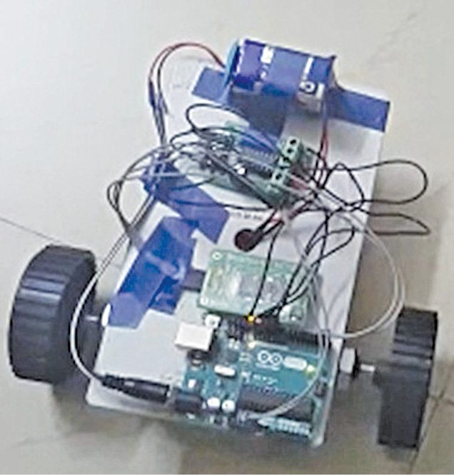


 To control a robot, the signal is usually sent through a wireless system using radio frequency (RF) and infrared (IR). To send an IR signal, you need a transmitter and a receiver with an encoding and decoding system. The simple circuit presented here can control the movement of a robot using an IR remote that is used for a TV or DVD player, or an equivalent IR remote.